Electronic component-embedded printed circuit board and method of manufacturing the same

a printed circuit board and electronic component technology, applied in the direction of printed circuit parts, printed circuit non-printed electric components association, printed circuit incorporation, etc., can solve the problems of limiting the degree of design freedom, affecting electrical performance, waste of entire printed circuit boards, etc., and achieve the effect of reducing component loss

Inactive Publication Date: 2013-05-02
SAMSUNG ELECTRO MECHANICS CO LTD
View PDF12 Cites 1 Cited by
  • Summary
  • Abstract
  • Description
  • Claims
  • Application Information

AI Technical Summary

Benefits of technology

[0014]The present invention has been invented in order to overcome the above-described problems and it is, therefore, an object of the present invention to provide an electronic component-embedded printed circuit board ca...

Problems solved by technology

In this case, a path of the circuit connecting the IC and the capacitor is increased by a thickness of the substrate to increase an impedance value, badly affecting electrical performance.
In addition, since a certain area of a lower end surface must be used for mounting a chip, for example, requirements of a user who wants a ball array disposed on the entire surface of the lower end cannot be satisfied, l...

Method used


Image

  • Electronic component-embedded printed circuit board and method of manufacturing the same
  • Electronic component-embedded printed circuit board and method of manufacturing the same
  • Electronic component-embedded printed circuit board and method of manufacturing the same

Examples


Embodiment Construction

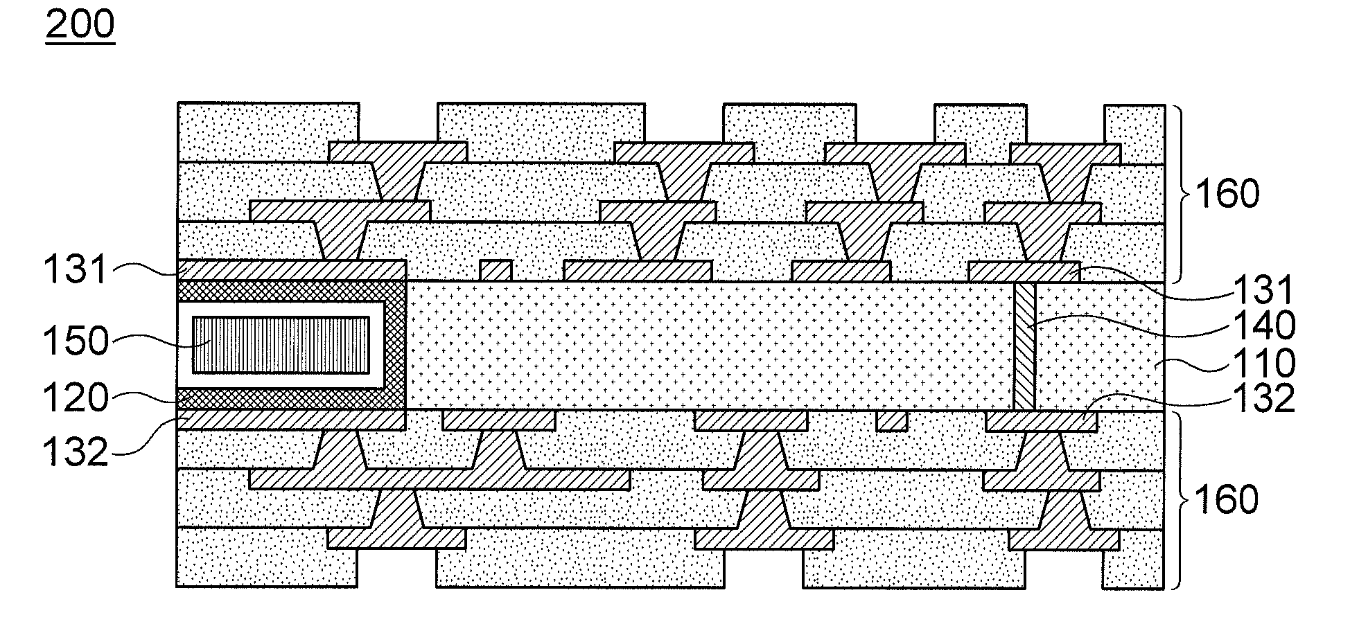
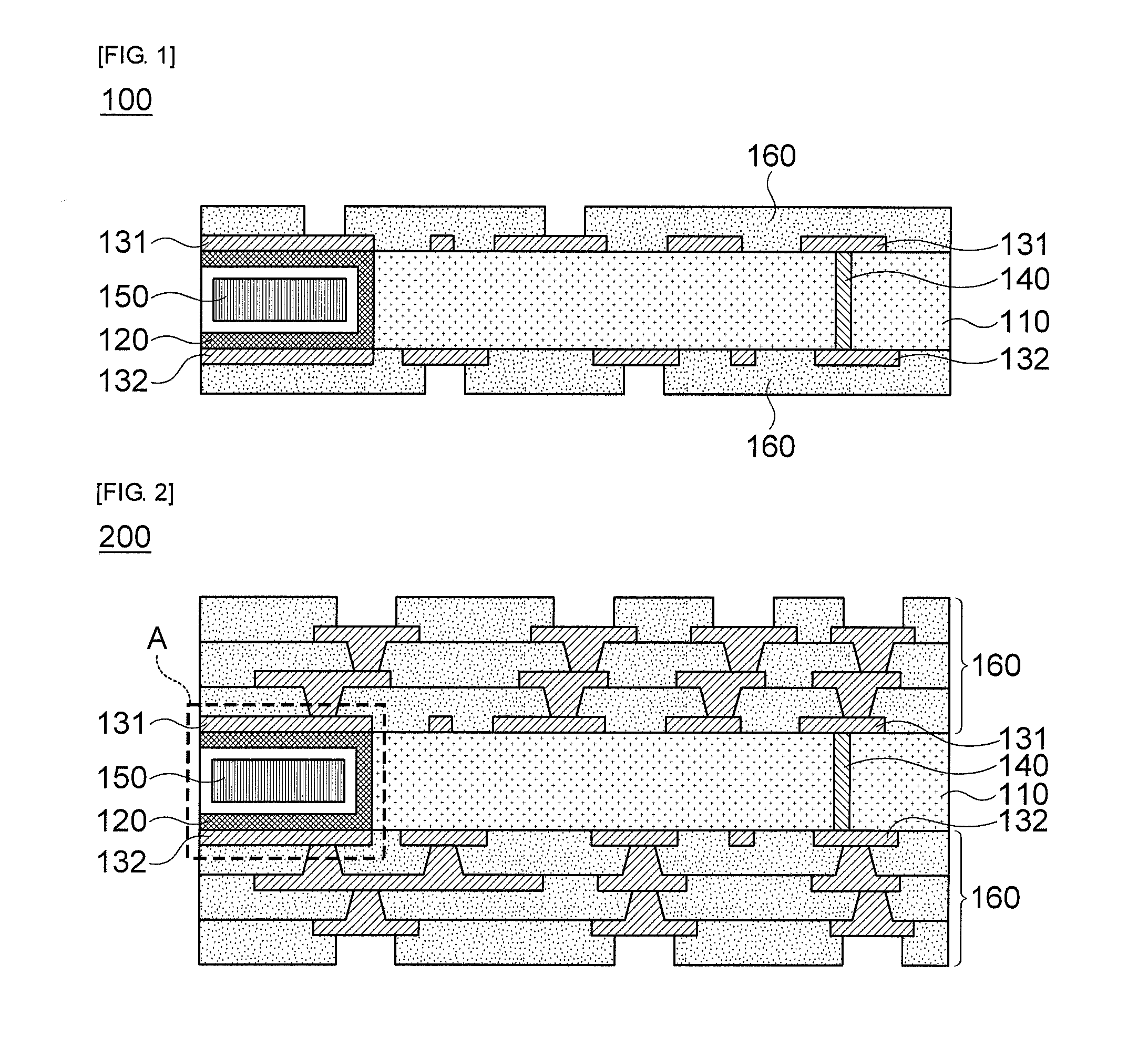
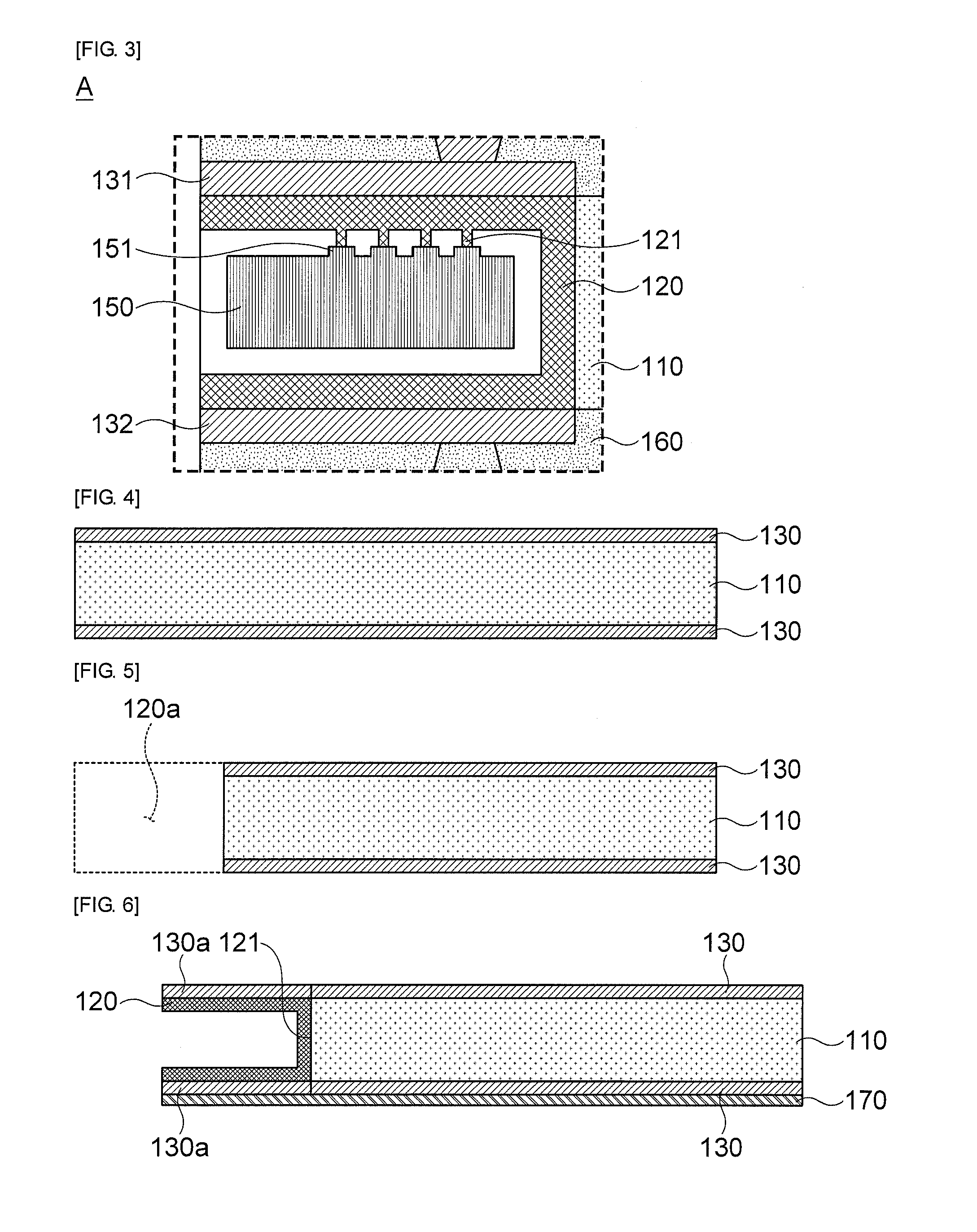
[0038]Hereinafter, a specific embodiment of the present invention will be described in detail with reference to the accompanying drawings. The following embodiments are provided as examples to fully convey the spirit of the invention to those skilled in the art.

[0039]Hereinafter, exemplary embodiments of the present invention will be described in detail. However, the present invention is not limited to the embodiments disclosed below but can be implemented in various forms. The following embodiments are described in order to enable those of ordinary skill in the art to embody and practice the present invention. To clearly describe the present invention, parts not relating to the description are omitted from the drawings.

[0040]The following embodiments are provided as examples to fully convey the spirit of the invention to those skilled in the art. Therefore, the present invention should not be construed as limited to the embodiments set forth herein and may be embodied in different ...


PUM

PropertyMeasurementUnit
aaaaaaaaaa

Abstract

An electronic component-embedded printed circuit board and a method of manufacturing the same. The printed circuit board includes a base substrate including a hollow electronic component case, an electronic component inserted into the electronic component case, circuit pattern layers formed on upper and lower surfaces of the base substrate, and an insulating layer formed to cover the circuit pattern layers. Accordingly, since the printed circuit board includes the electronic component case formed therein and the electronic component is inserted into only the printed circuit board, which has no defect after manufacture and final inspection of the printed circuit board, component loss due to yield of the printed circuit board can be reduced.

Description

CROSS-REFERENCE TO RELATED APPLICATIONS[0001]This application claims the benefit of Korean Patent Application No. 10-2011-0110473 filed with the Korea Intellectual Property Office on Oct. 27, 2011, the disclosure of which is incorporated herein by reference.BACKGROUND OF THE INVENTION[0002]1. Field of the Invention[0003]The present invention relates to an electronic component-embedded printed circuit board and a method of manufacturing the same, and more particularly, to an electronic component-embedded printed circuit board capable of reducing loss in substrate yield and enabling mass production and easy upgrade by detachably forming the electronic component embedded into the printed circuit board, and a method of manufacturing the same.[0004]2. Description of the Related Art[0005]According to market tendency requiring reduction in profile and various functions in a semiconductor package, various techniques are required to implement a printed circuit board.[0006]For example, in man...

Claims


Application Information

Patent Timeline
IPC IPC(8): H05K1/16H05K3/30
CPCH05K1/185Y10T29/49146H05K2201/10446H05K1/18H05K3/46
Inventor RYU, JONG INLEE, JIN WONCHUNG, YUL KYO
Owner SAMSUNG ELECTRO MECHANICS CO LTD
Why Eureka
Try Eureka