Vacuum processing device and method of transporting process subject member

Active Publication Date: 2013-05-02
HITACHI HIGH-TECH CORP
View PDF4 Cites 6 Cited by
  • Summary
  • Abstract
  • Description
  • Claims
  • Application Information

AI Technical Summary

Benefits of technology

The present invention provides a semiconductor processing device that is efficient in transporting different types of products in parallel process chambers. This device can improve transportation efficiency regardless of the number and arrangement of process chambers, the duration of the process in each chamber, and the overall process time. Additionally, the invention provides a vacuum processing device that can also ensure high transportation efficiency under various process conditions.

Problems solved by technology

However, the cluster tool device requires a large installation area, and in particular with an increase in diameters in recent years, the installation area has been becoming larger and larger.
At this time, when process time of a wafer to be transported next to a process chamber where a process has ended is long, although it may depend on the number and arrangement of process chambers in the semiconductor processing device, a transportation path for a wafer planned to be processed in a process chamber whose process time is short may be blocked, meaning that the wafer should have been transported to the process chamber beforehand.
Also, for this reason, a transportation control procedure of transporting wafers simply to process chambers starting in order with those where processes have ended earlier in a linear tool including a plurality of transportation robots has a problem that throughput is lowered in some cases depending on process time of wafers processed in each process chamber.

Method used


Image

  • Vacuum processing device and method of transporting process subject member
  • Vacuum processing device and method of transporting process subject member
  • Vacuum processing device and method of transporting process subject member

Examples


Embodiment Construction

[0041]Hereinafter, an embodiment of the present invention is explained with reference to drawings.

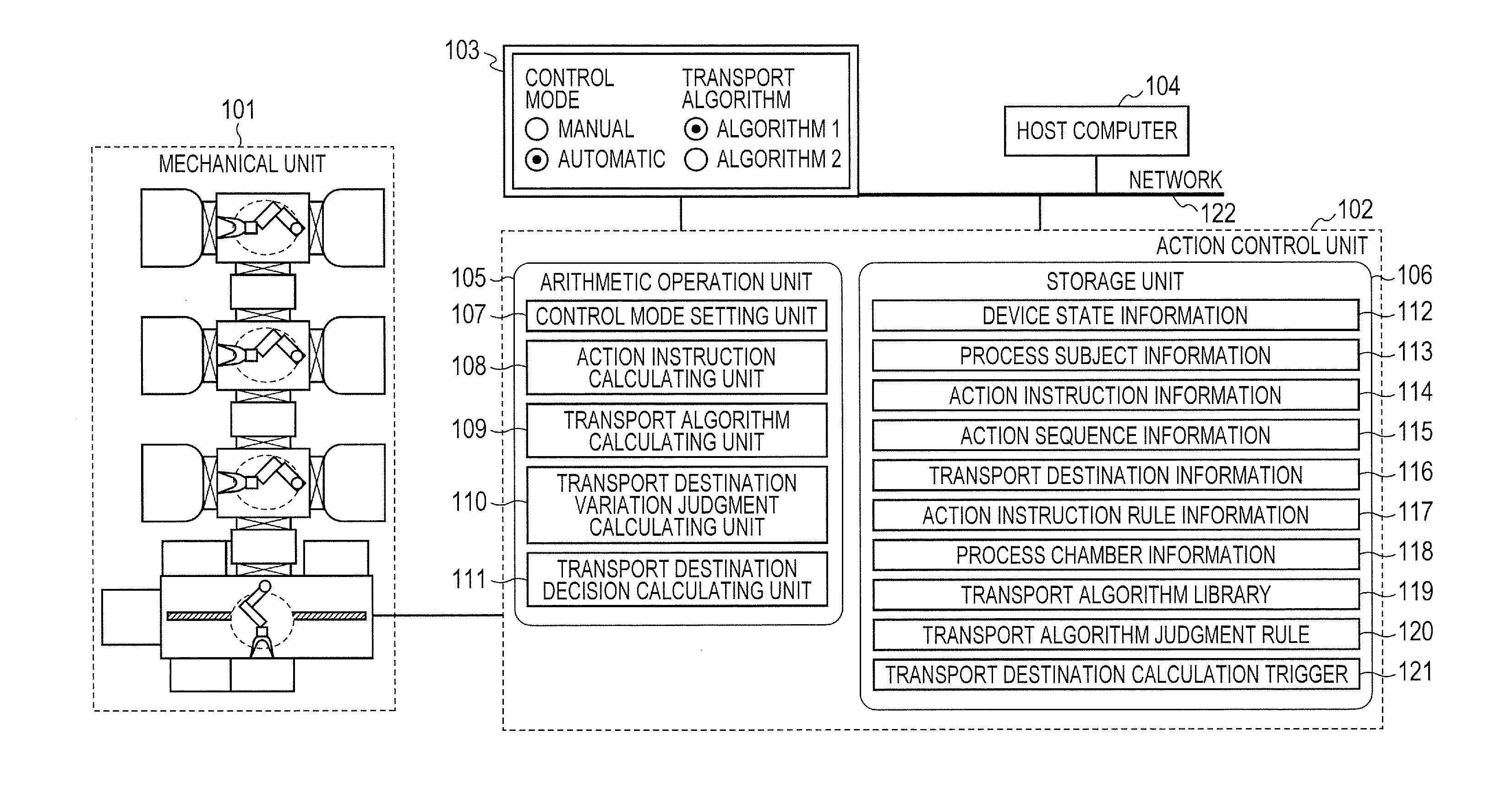
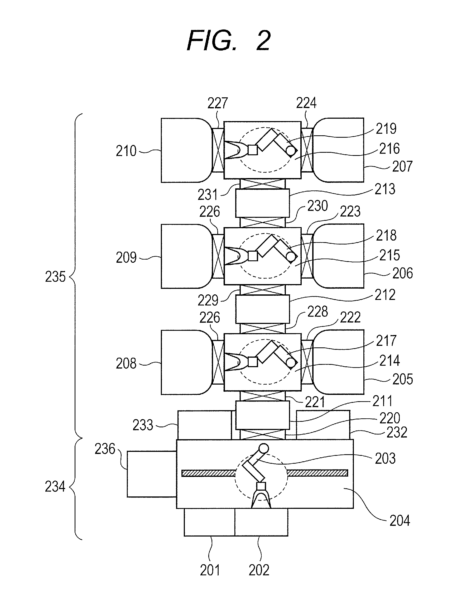
[0042]An outline of an overall configuration of a semiconductor processing device according to the present invention is explained with reference to FIG. 1. The semiconductor processing device is composed of, explaining roughly, a mechanical unit 101 including a process chamber and a transportation mechanism, an action control unit 102, and a console terminal 103. The mechanical unit 101 is configured with a process chamber that can perform processes such as etching and deposition on wafers, and a transportation mechanism included a robot and the like that performs transportation of the wafers. The action control unit 102 is a controller that controls actions of the process chamber and the transportation mechanism, and is composed of an arithmetic operation unit 105 that performs arithmetic operation processes and a storage unit 106 that stores various types of information.

[0043]The arit...


PUM


Abstract

Transportation control in a vacuum processing device with high transportation efficiency without lowering throughput is provided. A control unit is configured to update in real time and holds device state information showing an action state of each of a process chamber, a transportation mechanism unit, a buffer room, and a holding mechanism unit, the presence of a process subject member, and a process state thereof; select a transport algorithm from among transport algorithm judgment rules that are obtained by simulating in advance a plurality of transport algorithms for controlling transportation of a process subject member for each condition of a combination of the number and arrangement of the process chambers and process time of a process subject member based on the device state information and process time of the process subject member; and compute a transport destination of the process subject member based on the selected transport algorithm.

Description

CLAIM OF PRIORITY[0001]The present application claims priority from Japanese application serial no. JP2011-241068, filed on Nov. 2, 2011, the content of which is hereby incorporated by reference into this application.BACKGROUND OF THE INVENTION[0002]1) Field of the Invention[0003]The present invention relates to a vacuum processing device that is used to process a substrate-like wafer such as a semiconductor wafer and a liquid crystal display, and performs processes such as fine patterning using a plurality of types of gas, and a method of transporting a sample that is a process subject in the vacuum processing device.[0004]2) Description of the Related Art[0005]A vacuum processing device includes a processing unit including a vacuum container having a vacuum process chamber therein, an evacuation device, a plasma forming device and the like, and productivity is required to be improved with lower costs for such a vacuum processing device. It is an important task to make process effi...

Claims


Application Information

Patent Timeline
IPC IPC(8): H01L21/677
CPCH01L21/677H01L21/67276G05B19/41815G05B19/4189G05B2219/31002G05B2219/45031H01L21/67745
Inventor NOGI, KEITANAKATA, TERUOSUEMITSU, YOSHIROKAWAGUCHI, MICHINORIINOUE, SATOMI
Owner HITACHI HIGH-TECH CORP
Why Eureka
Try Eureka