Optical Tilted Charge Devices And Methods

a technology of tilted charge and charge device, which is applied in the direction of semiconductor/solid-state device manufacturing, semiconductor devices, electrical devices, etc., can solve the problems of transitioning from an optical tilted charge device to an optical tilted charge device design, and achieve the effect of high internal quantum efficiency

Inactive Publication Date: 2013-05-23
MELAKA MEDIA HOUSE
View PDF6 Cites 9 Cited by
  • Summary
  • Abstract
  • Description
  • Claims
  • Application Information

AI Technical Summary

Benefits of technology

[0010]The design of a practical optical tilted charge device includes several complex considerations including achievement of high internal quantum efficiency, manufacturability, compatibility and reliability. Therefore, transitioning from an existing design of an optical tilted charge device to another presents challenges. In accordance with an aspect of the present invention, there is provided an optical tilted charge device with a deep quantum well (with ΔE at least about 0.25 eV>>kT) while maintaining a heavily doped base region that is substantially binary. The optical tilted charge device with these features is still capable of incorporating etch stop layers that selectively stop etching at one type of semiconductor material, to assist in the definition of the emitter mesa, base mesa and collector mesa which benefits manufacturability. In addition, for reliability reasons, the base region can still be doped with carbon (p-type, NPN structure) or silicon (n-type, PNP). Compatibility is maintained, since the emission photon energies of the optical tilted charge device can still be coupled to existing InP / InGaAs based photodetectors. A further advantage is that the disclosed GaAs based optical tilted charge device hereof is compatible with the use of silicon-based substrates and lenses.

Problems solved by technology

Therefore, transitioning from an existing design of an optical tilted charge device to another presents challenges.

Method used


Image

  • Optical Tilted Charge Devices And Methods
  • Optical Tilted Charge Devices And Methods
  • Optical Tilted Charge Devices And Methods

Examples


Embodiment Construction

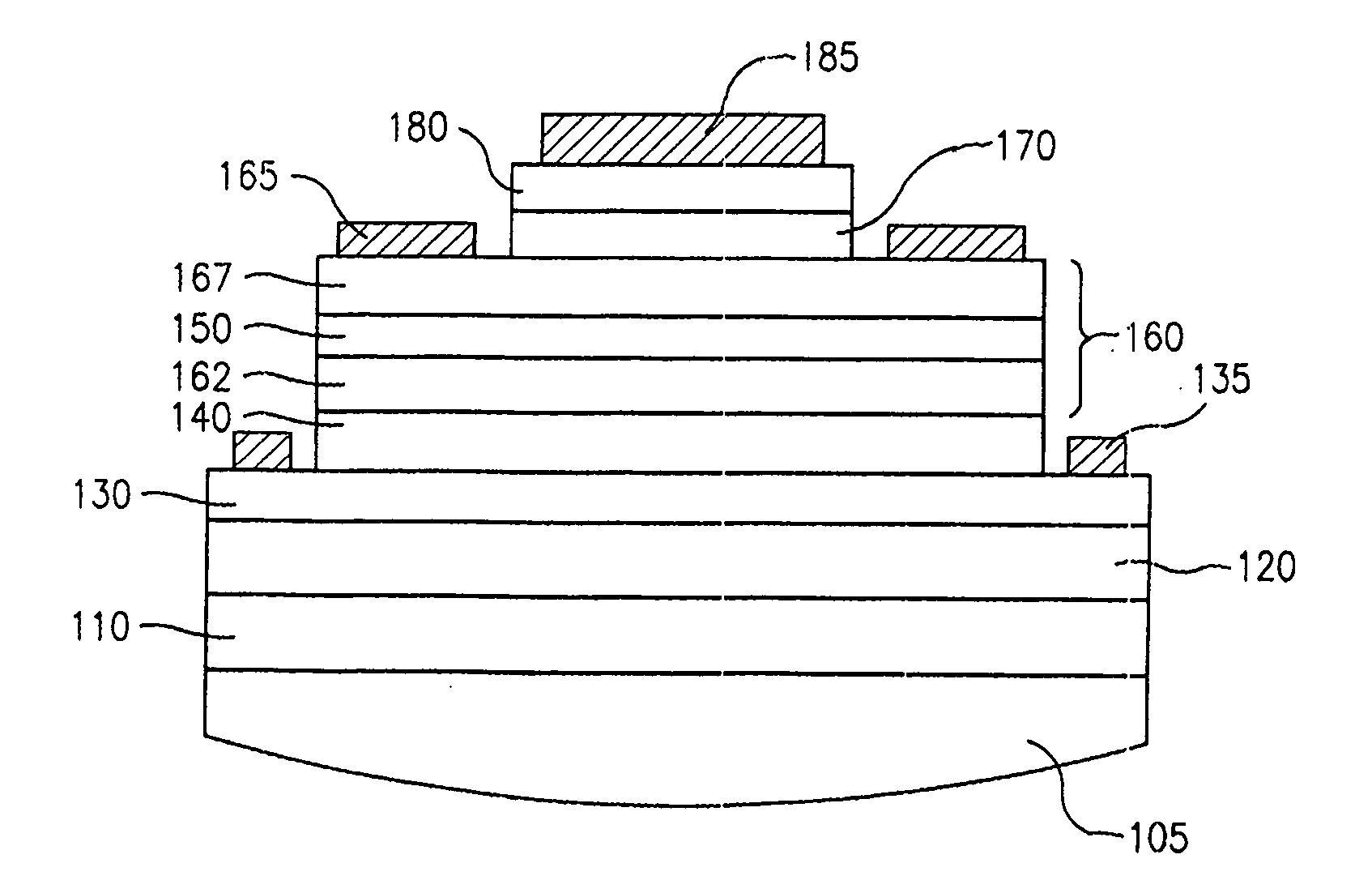
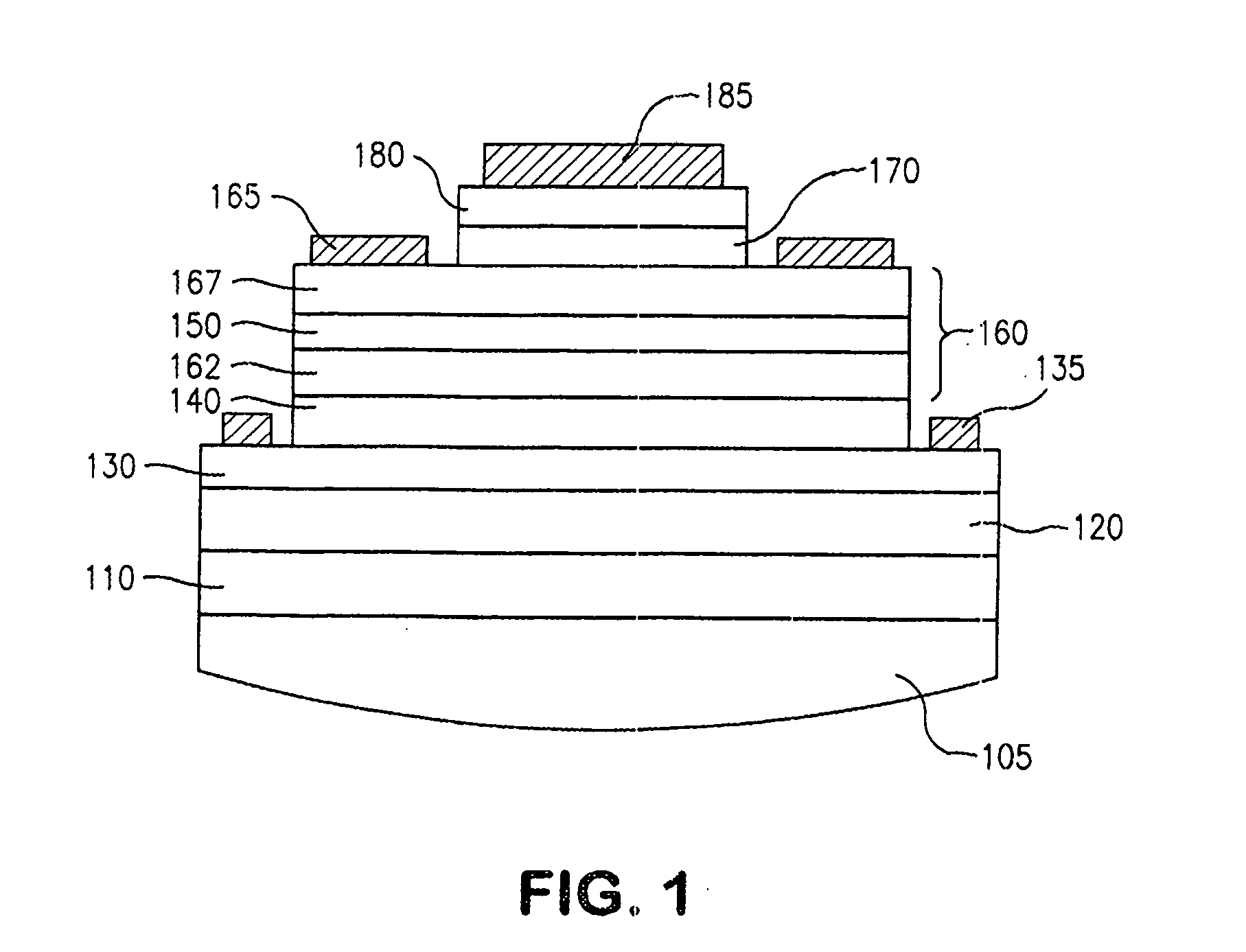
[0019]FIG. 1 shows a device in accordance with an embodiment of the invention, and which can be used in practicing an embodiment of the method of the invention. The semiconductor layering shown in FIG. 1, from the bottom up, includes: a GaAs substrate 110; a GaAs buffer region 120; a sub-collector region 130; a collector region 140; a base region 160 that includes a base sub-region 162 called “base-2”, a quantum size region 150 (one or more quantum wells or other suitable quantum size regions such as quantum dots or quantum wires), a base sub-region 167 called “base-1”, an emitter region 170, and a sub-emitter region 180. In accordance with a feature hereof, an InGaAsN quantum size region is employed in the base region. The collector, base, and emitter electrodes are shown respectively as metal collector contact 135 (which contacts the subcollector region), metal base contact 165 (which contacts the base-1 region), and metal emitter contact 185 (which contacts the sub-emitter region...


PUM


Abstract

A method for making an optical tilted-charge device that is substantially matched to GaAs lattice constant, including the following steps: providing a layered semiconductor structure that includes: a GaAs substrate; a semiconductor collector region; a semiconductor base region that includes a doped GaAs second base sub-region, an InGaAsN quantum size region, and a doped GaAs first base sub-region; and a semiconductor emitter region; and providing collector, base, and emitter electrodes respectively coupled with the collector region, the base region, and the emitter region. Electrical signals, applied with respect to the collector, base, and emitter electrodes, produces light emission from the base region.

Description

PRIORITY CLAIM[0001]Priority is claimed from U.S. Provisional Patent Application No. 61 / 629,181, filed Nov. 14, 2011, and said Provisional patent application is incorporated herein by reference.RELATED APPLICATION[0002]The subject matter of this application is related to subject matter of U.S. patent application Ser. No. ______, filed of even date herewith and assigned to the same assignee as the present application.FIELD OF THE INVENTION[0003]This invention relates to the field of semiconductor light emitting devices and techniques and, more particularly, to tilted charge light emitting devices and methods.BACKGROUND OF THE INVENTION[0004]Included in the background of the present invention are technologies relating to heterojunction bipolar transistors (HBTs, which are electrical tilted charge devices) and light-emitting transistors, transistor lasers, and tilted charge light-emitting diodes (respectively, LETs, TLs, and TCLEDs, all of which are optical tilted charge devices). A ti...

Claims


Application Information

Patent Timeline
Patent Type & Authority Applications(United States)
IPC IPC(8): H01L33/06H01L33/00
CPCH01L33/06H01L33/002H01L33/38H01L33/0075H01L33/0041
Inventor WALTER, GABRIEL
Owner MELAKA MEDIA HOUSE
Why Eureka
Try Eureka