Spectral Matching Based Calibration

Active Publication Date: 2013-05-23
KLA TENCOR CORP
View PDF14 Cites 13 Cited by
  • Summary
  • Abstract
  • Description
  • Claims
  • Application Information

AI Technical Summary

Benefits of technology

[0008]Methods and systems for calibrating system parameter values of a target inspection system are presented. The embodiments described herein generally relate to methods for increasing measurement consistency among inspection systems by minimizing the differences in the spectral error among different inspection systems for a given spec

Problems solved by technology

If measurement consistency among inspection systems degrades, consistency among processed semiconductor wafers is lost and yield drops to unacceptable levels.
This may be difficult to achieve in a manufacturing environment and lead to loss of consistency among inspection systems.
In addition, an expensive reference wafer set must be maintained in the manufacturing environment.
Risks of wafer breakage or degradation potentially jeopardize the integrity of the calibration process.
Moreover, the accuracy of an inspection system calibrated base

Method used


Image

  • Spectral Matching Based Calibration
  • Spectral Matching Based Calibration
  • Spectral Matching Based Calibration

Examples


Embodiment Construction

[0019]Reference will now be made in detail to background examples and some embodiments of the invention, examples of which are illustrated in the accompanying drawings.

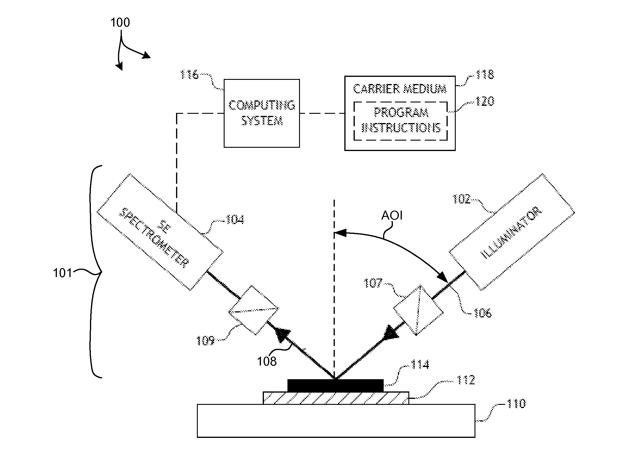
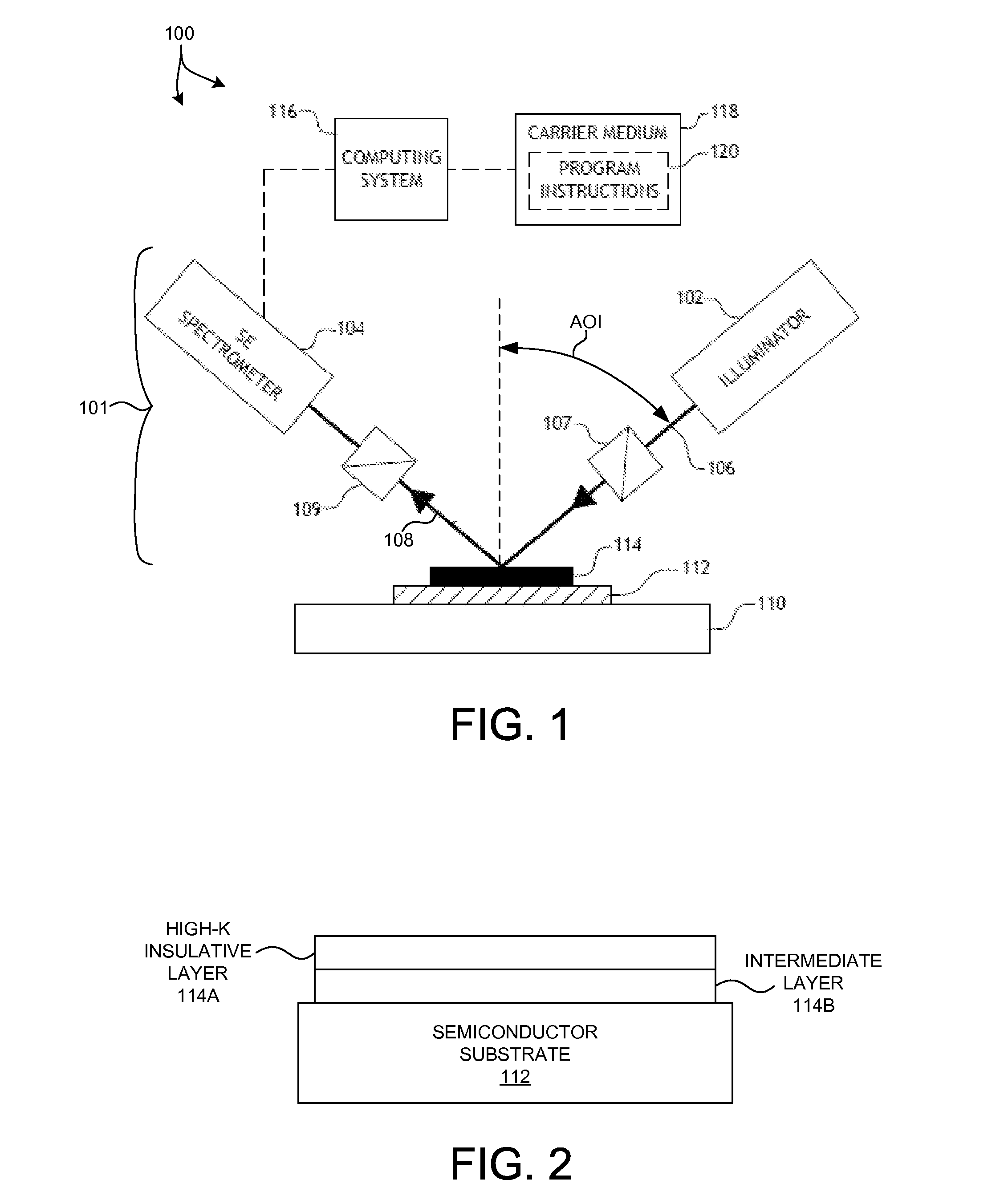
[0020]FIG. 1 illustrates a system 100 for measuring characteristics of a thin film of a semiconductor wafer in accordance with the exemplary methods presented herein. As shown in FIG. 1, the system 100 may be used to perform spectroscopic ellipsometry on one or more films 114 of a semiconductor wafer 112 disposed on a wafer positioning system 110. In this aspect, the system 100 may include a spectroscopic ellipsometer equipped with an illuminator 102 and a spectrometer 104. The illuminator 102 of the system 100 is configured to generate and direct illumination of a selected wavelength range (e.g., 150-850 nm) to the thin film (e.g., HfSiON thin film) disposed on the surface of the semiconductor wafer 112. In turn, the spectrometer 104 is configured to receive illumination reflected from the surface of the semiconducto...


PUM


Abstract

Methods and systems for calibrating system parameter values of a target inspection system are presented. Spectral Error Based Calibration (SEBC) increases consistency among inspection systems by minimizing differences in the spectral error among different inspection systems for a given specimen or set of specimens. The system parameter values are determined such that differences between a spectral error associated with a measurement of a specimen by the target inspection system and a spectral error associated with a measurement of the same specimen by a reference inspection system are minimized. In some examples, system parameter values are calibrated without modifying specimen parameters. Small inaccuracies in specimen parameter values have little effect on the calibration because the target system and the reference system both measure the same specimen or set of specimens. By performing SEBC over a set of specimens, the resulting calibration is robust to a wide range of specimens under test.

Description

CROSS REFERENCE TO RELATED APPLICATION[0001]The present application for patent claims priority under 35 U.S.C. §119 from U.S. provisional patent application Ser. No. 61 / 562,154, entitled “Spectral Matching Based Calibration,” filed Nov. 21, 2011, the subject matter of which is incorporated herein by reference.TECHNICAL FIELD[0002]The described embodiments relate to systems for wafer inspection, and more particularly to characterization and defect detection of thin films used in semiconductor manufacturing.BACKGROUND INFORMATION[0003]Semiconductor devices such as logic and memory devices are typically fabricated by a sequence of processing steps applied to a substrate or wafer. The various features and multiple structural levels of the semiconductor devices are formed by these processing steps. For example, lithography among others is one semiconductor fabrication process that involves generating a pattern on a semiconductor wafer. Additional examples of semiconductor fabrication pro...

Claims


Application Information

Patent Timeline
IPC IPC(8): G01N21/27
CPCG01N21/274G03F7/70608G01N21/211
Inventor KWAK, HIDONGJIANG, ZHIMINGDIXON, WARD RDELLJAMES, JR., KENNETH EDWARDPOSLAVSKY, LEONIDKAACK, TORSTEN
Owner KLA TENCOR CORP
Why Eureka
Try Eureka