Radiation-Emitting Semiconductor Body, Method for Producing a Radiation-Emitting Semiconductor Body and Radiation-Emitting Semiconductor Component

Active Publication Date: 2013-05-30
OSRAM OLED
View PDF0 Cites 4 Cited by
  • Summary
  • Abstract
  • Description
  • Claims
  • Application Information

AI Technical Summary

Benefits of technology

[0005]In one aspect, the present invention provides a semiconductor body which is suitable for being applied onto a chip carrier by a bonding method, in particular ultrasound-friction welding or thermocompression. In a further asp

Problems solved by technology

This production method is comparatively time-co

Method used


Image

  • Radiation-Emitting Semiconductor Body, Method for Producing a Radiation-Emitting Semiconductor Body and Radiation-Emitting Semiconductor Component
  • Radiation-Emitting Semiconductor Body, Method for Producing a Radiation-Emitting Semiconductor Body and Radiation-Emitting Semiconductor Component
  • Radiation-Emitting Semiconductor Body, Method for Producing a Radiation-Emitting Semiconductor Body and Radiation-Emitting Semiconductor Component

Examples


Embodiment Construction

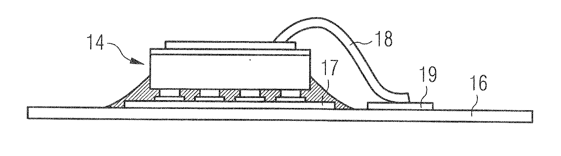
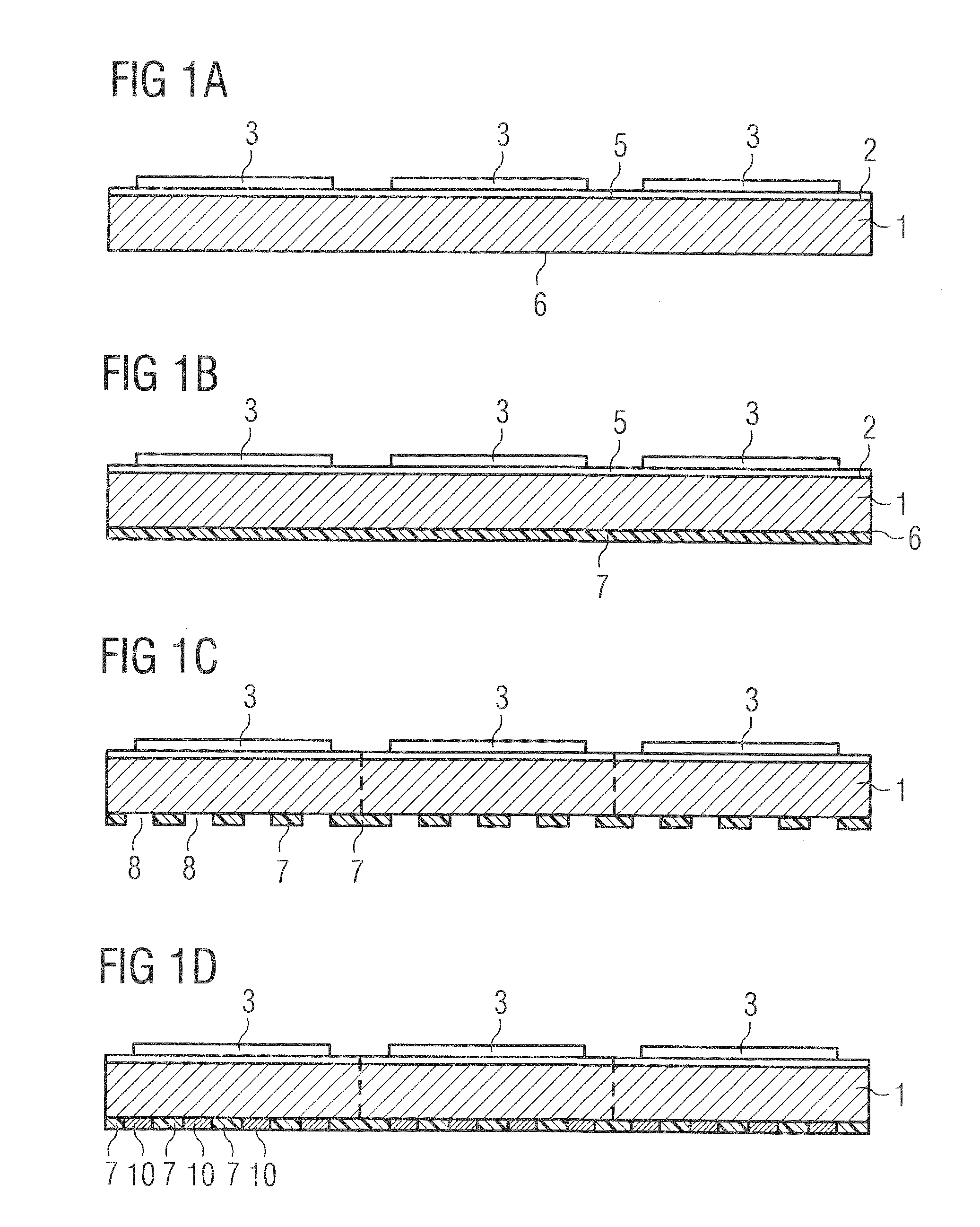
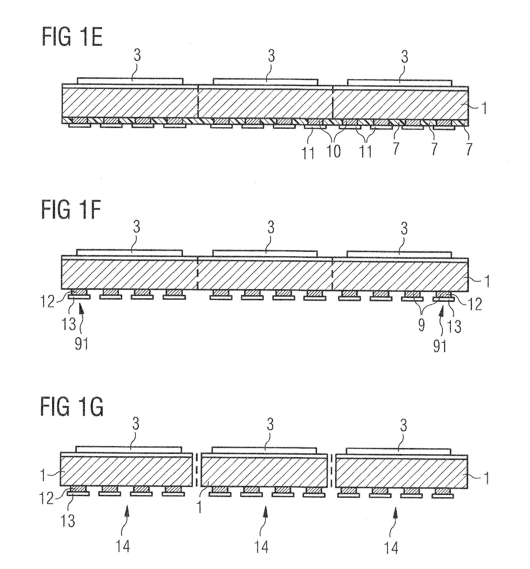
[0046]FIG. 1A shows a carrier layer 1, on the first main side 2 of which an epitaxial semiconductor layer sequence 3 is arranged. The carrier layer 1 mechanically stabilizes the semiconductor layer sequence 3. The epitaxial semiconductor layer sequence 3 in the present case is already structured into chip regions, of which each chip region is subsequently part of a finished semiconductor body. The epitaxial semiconductor layer sequence 3 has an active zone 4 (not represented in FIGS. 1A to 1G), which is suitable for generating electromagnetic radiation.

[0047]Particularly preferably, the further layer 10 is formed so as to be metallic and comprises the same material as the carrier layer 1, for example nickel, molybdenum, copper.

[0048]The carrier layer 1 in the present case is formed so as to be metallic and comprises for example nickel, molybdenum, copper.

[0049]The active zone 4 preferably comprises a pn junction, a double heterostructure, a single quantum well or particularly prefer...


PUM


Abstract

A radiation-emitting semiconductor body is provided which, besides an epitaxial semiconductor layer sequence having an active zone that is suitable for generating electromagnetic radiation, has a carrier layer that is intended to mechanically stabilize the epitaxial semiconductor layer sequence. The semiconductor body furthermore has contact structures for electrical contacting of the semiconductor body, which respectively have a volume region and a surface bonding region. The surface bonding region is formed from a material which is different from the material of the volume region.

Description

[0001]This patent application is a national phase filing under section 371 of PCT / EP2011 / 059485, filed Jun. 8, 2011, which claims the priority of German patent application 10 2010 023 343.9, filed Jun. 10, 2010, each of which is incorporated herein by reference in its entirety.TECHNICAL FIELD[0002]The invention relates to a radiation-emitting semiconductor body, to a method for producing a radiation-emitting semiconductor body and to a radiation-emitting semiconductor component.BACKGROUND[0003]Document EP 1 657 757 A2 describes a radiation-emitting semiconductor component comprising a radiation-emitting semiconductor body, which is applied electrically conductively onto a chip carrier by a bonding method, for example ultrasound-friction welding or thermocompression, via backside electrical contacts.[0004]In order to produce the backside contacts, individual conductive contacts are applied successively onto the semiconductor body with the aid of a ball bonder, as described for exampl...

Claims


Application Information

Patent Timeline
IPC IPC(8): H01L33/40
CPCH01L24/73H01L33/40H01L33/387H01L33/62H01L2224/48091H01L2924/01013H01L2924/01029H01L2924/01079H05K2201/10106H05K2201/10969H01L33/0079H01L2924/01068H01L2924/01042H01L2924/00014H01L2924/12042H01L2924/12036H01L2933/0066H01L2224/92125H01L2224/92227H01L2224/73204H01L2224/16225H01L2224/32225H01L33/0093H01L2924/00H01L33/36H01L33/38
Inventor BRUNNER, HERBERTNINZ, PATRICK
Owner OSRAM OLED
Why Eureka
Try Eureka