Alloyed 2N Copper Wires for Bonding in Microelectronics Devices
- Summary
- Abstract
- Description
- Claims
- Application Information
AI Technical Summary
Benefits of technology
Problems solved by technology
Method used
Image

Examples
Embodiment Construction
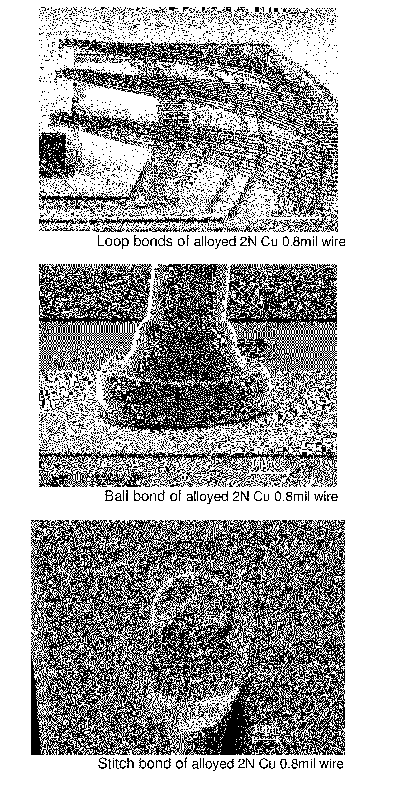
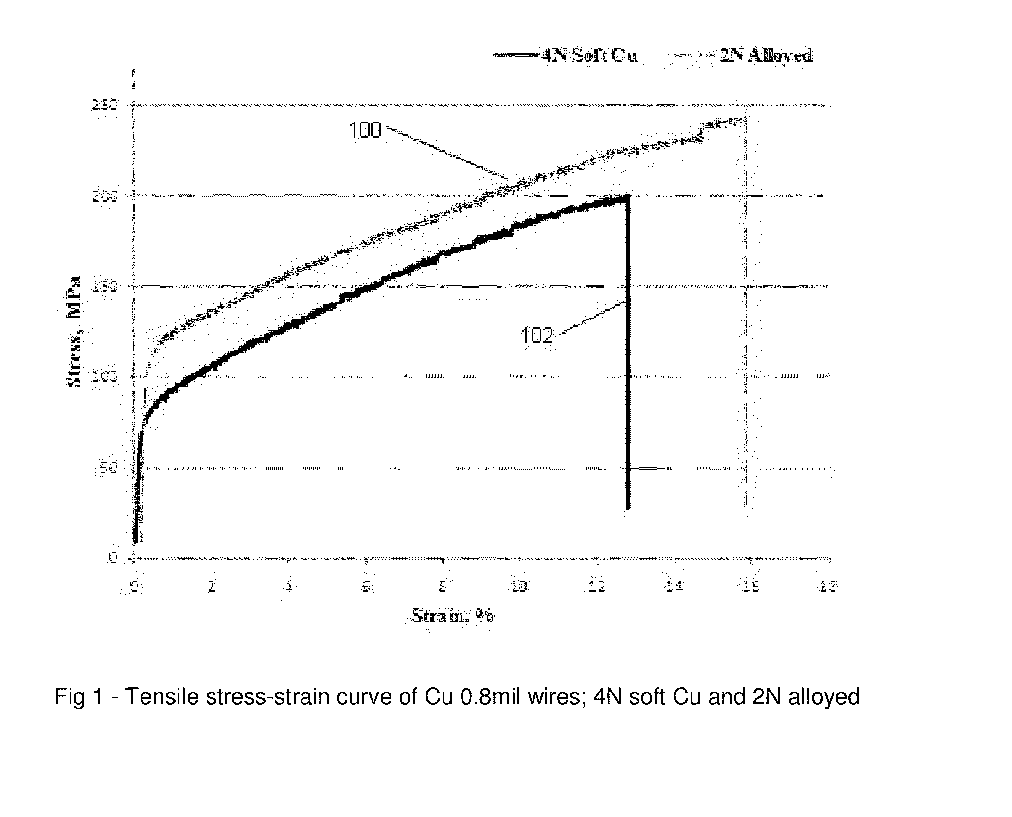
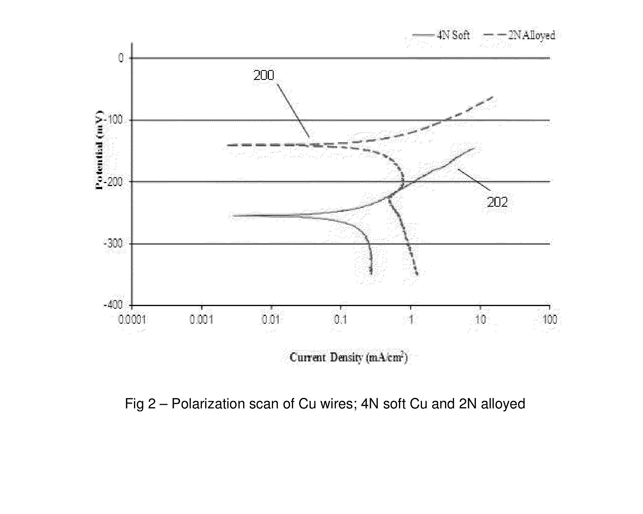
[0034]The example embodiments described herein provide alloyed 2N Cu wires for bonding in microelectronics packaging industries. The wires are prepared using high purity Cu (>99.99%) and as major alloying elements Ag, Ni, Pd, Au, Pt, Cr, Ca, Ce, Mg, La, Al, P, Fe, B, Zr and Ti. Fine wires are drawn from the alloyed Cu. The wires in example embodiments are bondable to Al bond pads, as well as Ag, Cu, Au, Pd plated surfaces. The results of HTS (high temperature storage) of the wire bonds are comparable to a commercially available 4N soft Cu reference wire, when bonded to an Al bond pad and stored at about 175° C. for about 1000 hours. Corrosion resistance of the alloyed wires is advantageously better than the 4N soft Cu reference wire. As will be appreciated by a person skilled in the art, HAST or THB (temperature humidity bias) tests are typically conducted for Cu wire bonded and epoxy molded devices using biased or unbiased conditions. During the test, the Cu wire bond interface (i....
PUM
| Property | Measurement | Unit |
|---|---|---|
| Force | aaaaa | aaaaa |
| Corrosion resistance | aaaaa | aaaaa |
Abstract
Description
Claims
Application Information
 - Generate Ideas
- Intellectual Property
- Life Sciences
- Materials
- Tech Scout
- Unparalleled Data Quality
- Higher Quality Content
- 60% Fewer Hallucinations
Browse by: Latest US Patents, China's latest patents, Technical Efficacy Thesaurus, Application Domain, Technology Topic, Popular Technical Reports.
© 2025 PatSnap. All rights reserved.Legal|Privacy policy|Modern Slavery Act Transparency Statement|Sitemap|About US| Contact US: help@patsnap.com