
Testing device for force-electricity property under nanowire original position stretching in transmission electron microscope

A technology of in-situ stretching and transmission electron microscopy, applied in the direction of measuring devices, strength characteristics, and material analysis through electromagnetic means, can solve the problem of inability to quantify the elastic coefficient, fail to satisfy nanomaterials, and fail to meet the electrical properties of a single one-dimensional nanomaterial Measurement and other issues, to achieve the effect of reliable performance, wide application range and simple structure

Inactive Publication Date: 2008-01-23
BEIJING UNIV OF TECH
View PDF0 Cites 35 Cited by
  • Summary
  • Abstract
  • Description
  • Claims
  • Application Information

AI Technical Summary

Problems solved by technology

Although this method can effectively give information on the atomic scale, it cannot quantify the elastic coefficient of a single one-dimensional nanomaterial
[0008] None of the above methods can measure the electrical properties of a single one-dimensional nanomaterial under stress, and can no longer meet the current requirements for testing the mechanical properties, electrical properties, and mechanical-electrical coupling performance of nanomaterials on the microscopic scale.

Method used


Image

  • Testing device for force-electricity property under nanowire original position stretching in transmission electron microscope
  • Testing device for force-electricity property under nanowire original position stretching in transmission electron microscope

Examples


Embodiment Construction

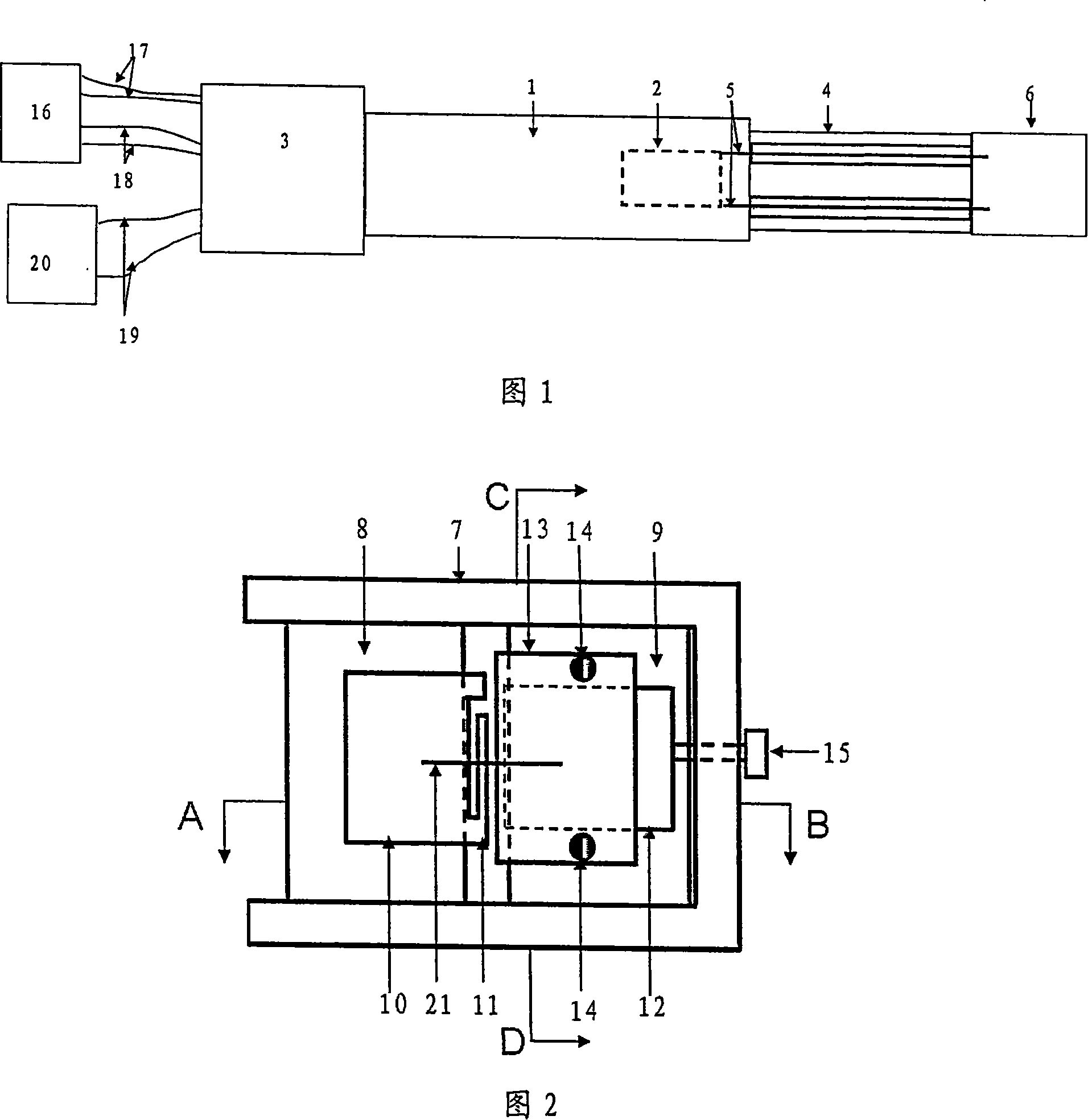
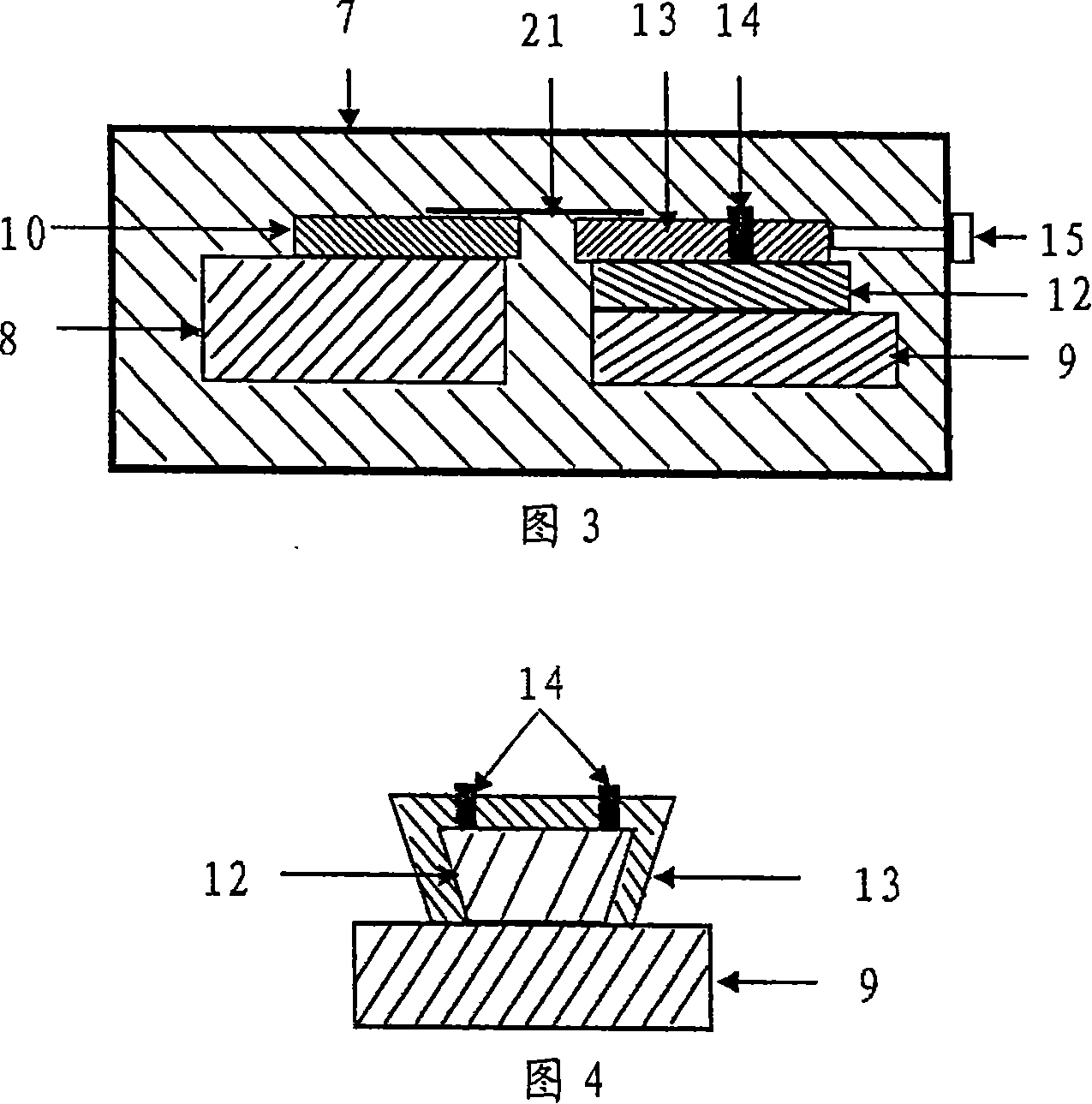
[0026] As shown in Figure 1, the piezoelectric ceramic sheet 2 is placed in the sealed tube 1 of the sample rod, and its inner end is fixed on the sealed tube 1 of the sample rod, and one end of the two driving wires 19 is connected to the piezoelectric ceramic sheet 2 positive and negative poles, and the other end is externally connected to the driving power supply 20. The connecting rod 5 is a rigid material, placed in the groove of the bearing base 4, one end of the connecting rod 5 is fixedly connected with the outer end of the piezoelectric ceramic sheet 2, and the other end of the connecting rod 5 is connected to the integrated block 6 by screws. The metal slider 13 is connected. The ends of the two loading wires 17 and the two signal wires 18 are connected to the gold-plated silicon chip 10 and the metal slider 13 on the integrated block 6 and are detachable. The other end of the driving wire 19, the loading wire 17 and the signal wire 18 are drawn from the outer end o...


PUM


Abstract

The invention provides a mechanic-electric property tester for in-situ tensioning of nanometer line in a transmission electron microscopy (TEM), pertains to the in-situ testing of properties of nanometer material. The invention comprises a piezoelectric ceramic tensile unit, a micro cantilever beam mechanics testing system and an electric measuring system, and carries out in-situ tensioning for a single nanometer line and other nanometer materials in a TEM, and realizes an imaging system that can take use of the TEM during the tensioning, so as to get in-situ deformation in nanometer size or atom size. In addition, the invention can achieve quantitative measurement on such mechanical properties as elasticity, plasticity and breakage, and also can carry out measurement on electric properties of a lot of nanometer materials, and investigate the property for transmitting electric charges during the tensioning. The invention is of simple structure, easy to operate, widely applicable, is straightforward and quantitative, is good for explaining and discovering the excellent comprehensive properties of nanometer materials in term of mechanics and electrics.

Description

Technical field: [0001] The invention belongs to the field of in-situ detection of properties of nanometer materials. Background technique: [0002] Realizing the manipulation and in-situ performance measurement of monomeric nanostructures is a key scientific and technological issue that is the bottleneck in the research of new nanostructures, new properties and new devices, especially in the transmission electron microscope, due to its narrow space, people It is more difficult to realize the test of the single nanostructure. [0003] It should be pointed out that although people have conducted in-depth studies on the mechanical and electrical properties of monomeric nanomaterials in recent years, due to their difficulty and complexity, no accepted conclusions have been formed so far. One-dimensional nanomaterials are used as interconnect lines or basic functional units of micro-electromechanical systems and nano-electromechanical systems. Therefore, fully understanding the...

Claims


Application Information

Patent Timeline
IPC IPC(8): G01N13/10G01N3/00G01N27/00G01Q60/10
Inventor 韩晓东郑坤张泽
Owner BEIJING UNIV OF TECH
Learn More