Semiconductor device having skew detection circuit measuring skew between clock signal and data strobe signal

Inactive Publication Date: 2013-06-06
LONGITUDE SEMICON S A R L
View PDF1 Cites 48 Cited by
  • Summary
  • Abstract
  • Description
  • Claims
  • Application Information

AI Technical Summary

Problems solved by technology

However, the write data fetched by the semiconductor memory device is transferred to a memory cell array synchronously with a clock signal, which is different from the data strobe signal.
Therefore, when a skew exists between the data strobe signal and the clock signal, a write operation may not be performed correctly.
However, the DLL circuit is a circuit block that consumes a relatively large amount of power.
Therefore, the DLL circuit may not be provided in a semiconductor memor

Method used


Image

  • Semiconductor device having skew detection circuit measuring skew between clock signal and data strobe signal
  • Semiconductor device having skew detection circuit measuring skew between clock signal and data strobe signal
  • Semiconductor device having skew detection circuit measuring skew between clock signal and data strobe signal

Examples


Embodiment Construction

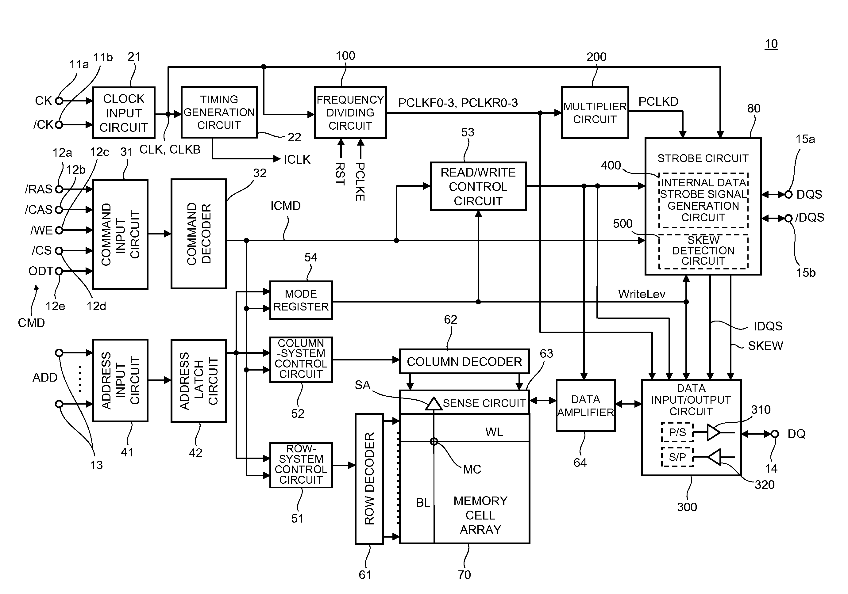
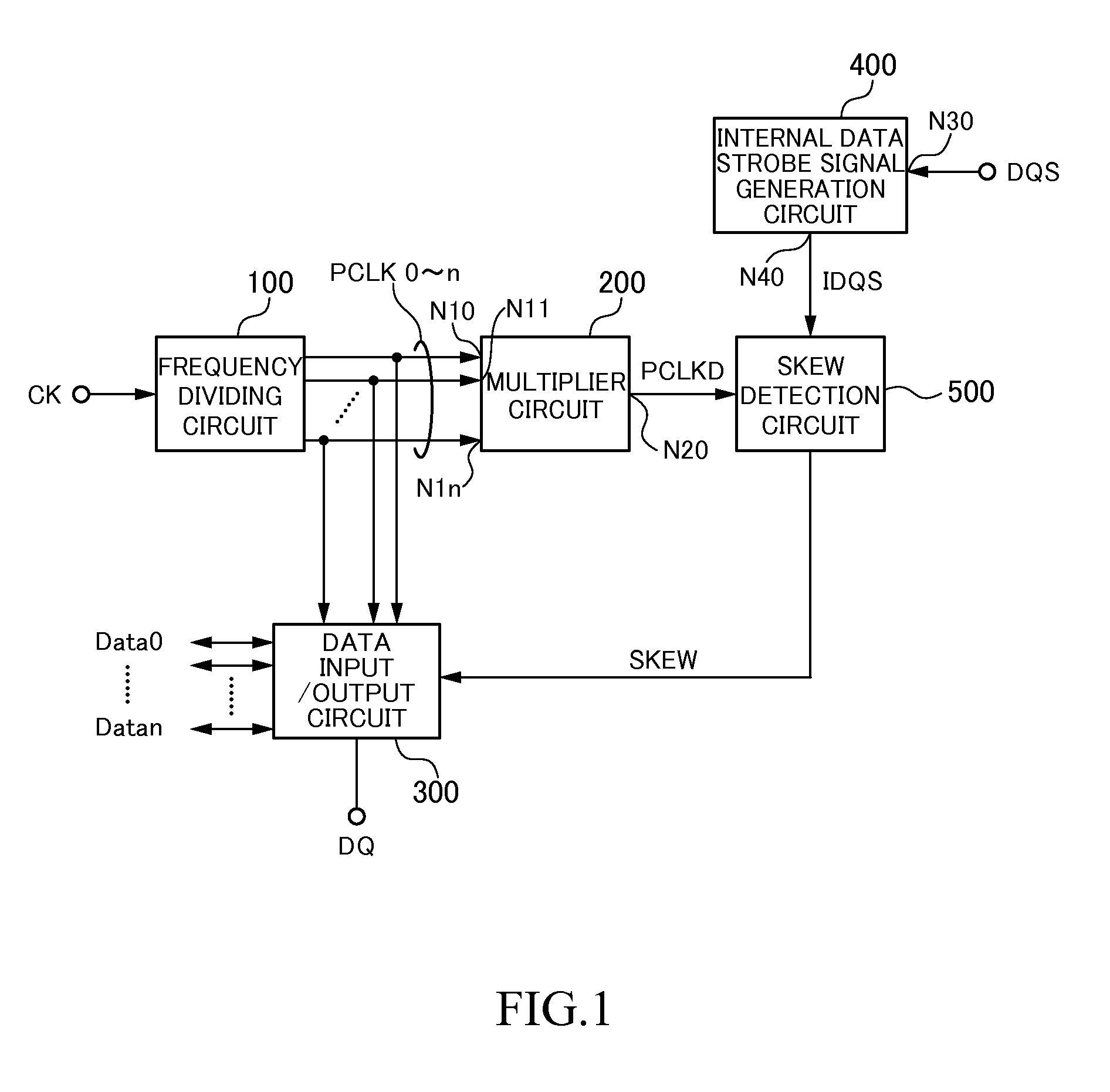
[0030]One embodiment of the present invention will be described below. However, the claims of the present application are not limited to the embodiment. That is, according to one embodiment of the present invention, a semiconductor device includes: a multiplier circuit that multiplies a plurality of frequency-divided clock signals to generate an internal clock signal; an internal data strobe signal generation circuit that generates an internal data strobe signal based on an external data strobe signal; and a skew detection circuit that detects skew between the internal clock signal and the internal data strobe signal, wherein an amount of delay that the multiplier circuit has is substantially equal to an amount of delay that the internal data strobe signal generation circuit has. As a result, an offset of a write leveling operation that is attributable to the amount of delay by the multiplier circuit is cancelled. Therefore, the accurate write leveling operation is possible.

[0031]Re...


PUM


Abstract

Disclosed herein is a semiconductor device that includes a clock terminal supplied with a first clock signal from outside; a dividing circuit dividing a frequency of the first clock signal to generate a plurality of second clock signals that are different in phase from one another; a multiplier circuit multiplying the second clock signals to generate a third clock signal, the multiplexer having a predetermined operating delay time; a data strobe terminal supplied with a first data strobe signal from outside; a strobe signal generation circuit adding the predetermined operating delay time to the first data strobe signal to generate a second data strobe signal; and a skew detection circuit measuring a skew between the third clock signal and the second data strobe signal.

Description

BACKGROUND OF THE INVENTION[0001]1. Field of the Invention[0002]The present invention relates to a semiconductor device, and more particularly relates to a semiconductor device having a skew detection circuit measuring a skew between a clock signal and a data strobe signal.[0003]2. Description of Related Art[0004]Transmission and reception of read data and write data between a semiconductor memory device such as a DRAM (Dynamic Random Access Memory) and a memory controller may be performed synchronously with a data strobe signal. For example, in a write operation, a memory controller supplies a data strobe signal and write data to a semiconductor memory device, and the semiconductor memory device fetches the write data synchronously with the data strobe signal.[0005]However, the write data fetched by the semiconductor memory device is transferred to a memory cell array synchronously with a clock signal, which is different from the data strobe signal. Therefore, when a skew exists be...

Claims


Application Information

Patent Timeline
IPC IPC(8): G11C7/22
CPCG11C7/22G11C7/222G11C7/1093G11C7/10
Inventor ITO, KOJIMATSUI, YOSHINORI
Owner LONGITUDE SEMICON S A R L
Why Eureka
Try Eureka