Metal-contamination-free through-substrate via structure

a technology of through-substrate and metal contamination, which is applied in the direction of semiconductor/solid-state device details, semiconductor devices, electrical apparatus, etc., can solve the problems that the diffusion of residual copper material into the semiconductor material can create detrimental effects, and the silica oxide dielectric liner does not prevent the diffusion of metallic materials

Active Publication Date: 2013-06-06
GLOBALFOUNDRIES U S INC
View PDF6 Cites 7 Cited by
  • Summary
  • Abstract
  • Description
  • Claims
  • Application Information

AI Technical Summary

Benefits of technology

[0005]A through-substrate via (TSV) structure that is immune to metal contamination due to a backside planarization process is provided. After forming a through-substrate via (TSV) trench, a diffusion barrier liner is conformally deposited on the sidewalls of the TSV trench. A dielectric liner is formed by depositing a dielectric material on vertical portions of the diffusion barrier liner. A metallic conductive via structure is formed by subsequently filling the TSV trench. Horizontal portions of the diffusion barrier liner can be removed by an anisotropic etch prior to deposition of a conductive material for the metallic conductive via structure, or can be removed by planarization after removing the horizontal portion of the dielectric liner. The diffusion barrier liner protects the semiconductor material of the substrate during the backside planarization by blocking residual metallic material originating from the metallic conductive via structure from entering into the semiconductor material of the substrate, thereby protecting the semiconductor devices within the substrate from metallic contamination.

Problems solved by technology

The silicon oxide dielectric liner does not prevent metallic materials from diffusing through.
Diffusion of such residual copper material into the semiconductor material can create detrimental effects such as electrical shorts within semiconductor devices in the substrate.

Method used


Image

  • Metal-contamination-free through-substrate via structure
  • Metal-contamination-free through-substrate via structure
  • Metal-contamination-free through-substrate via structure

Examples


Embodiment Construction

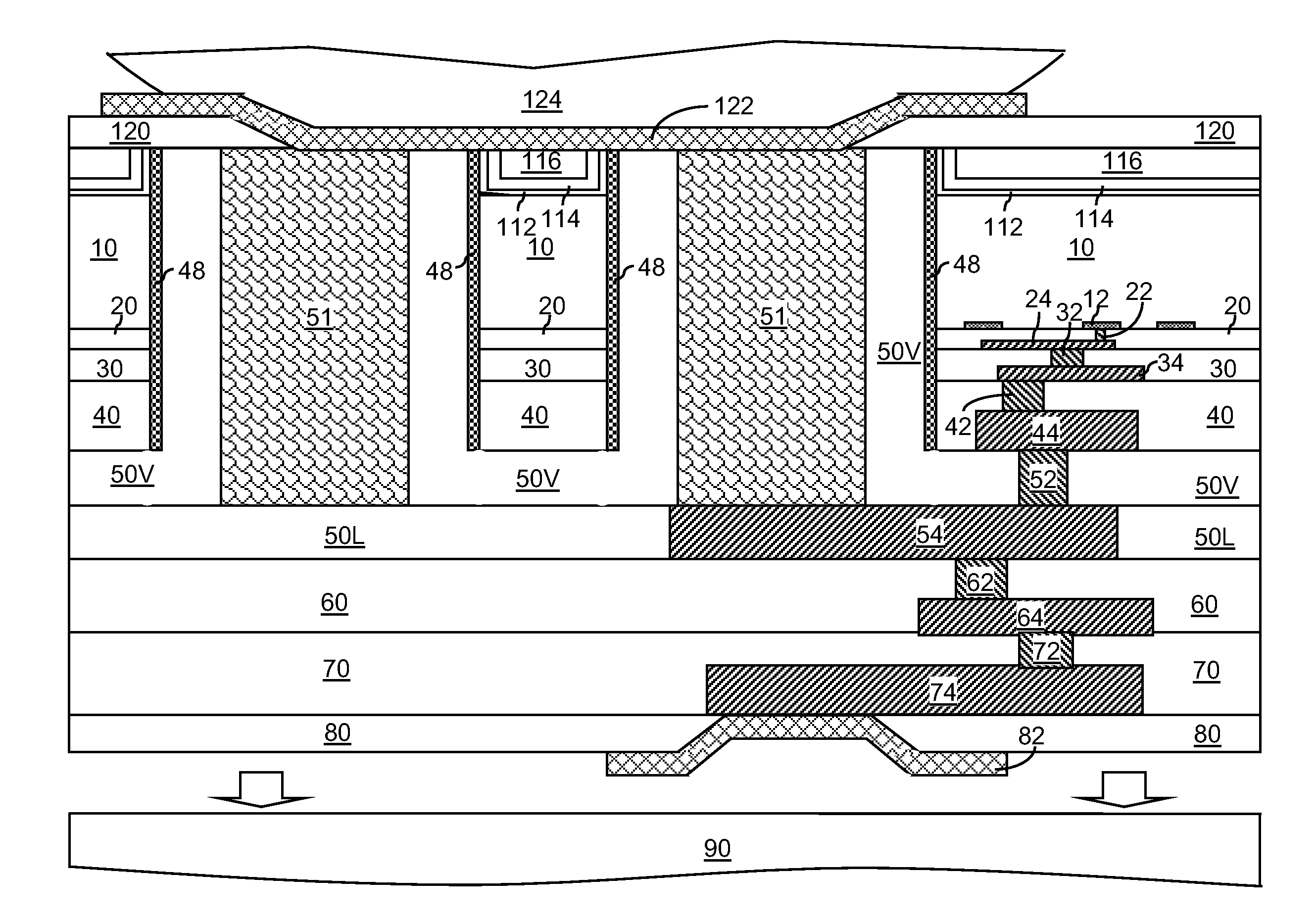
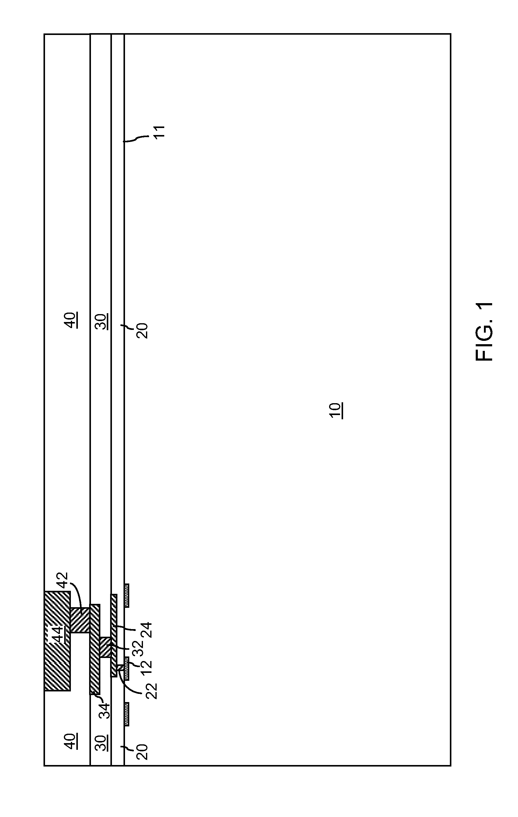
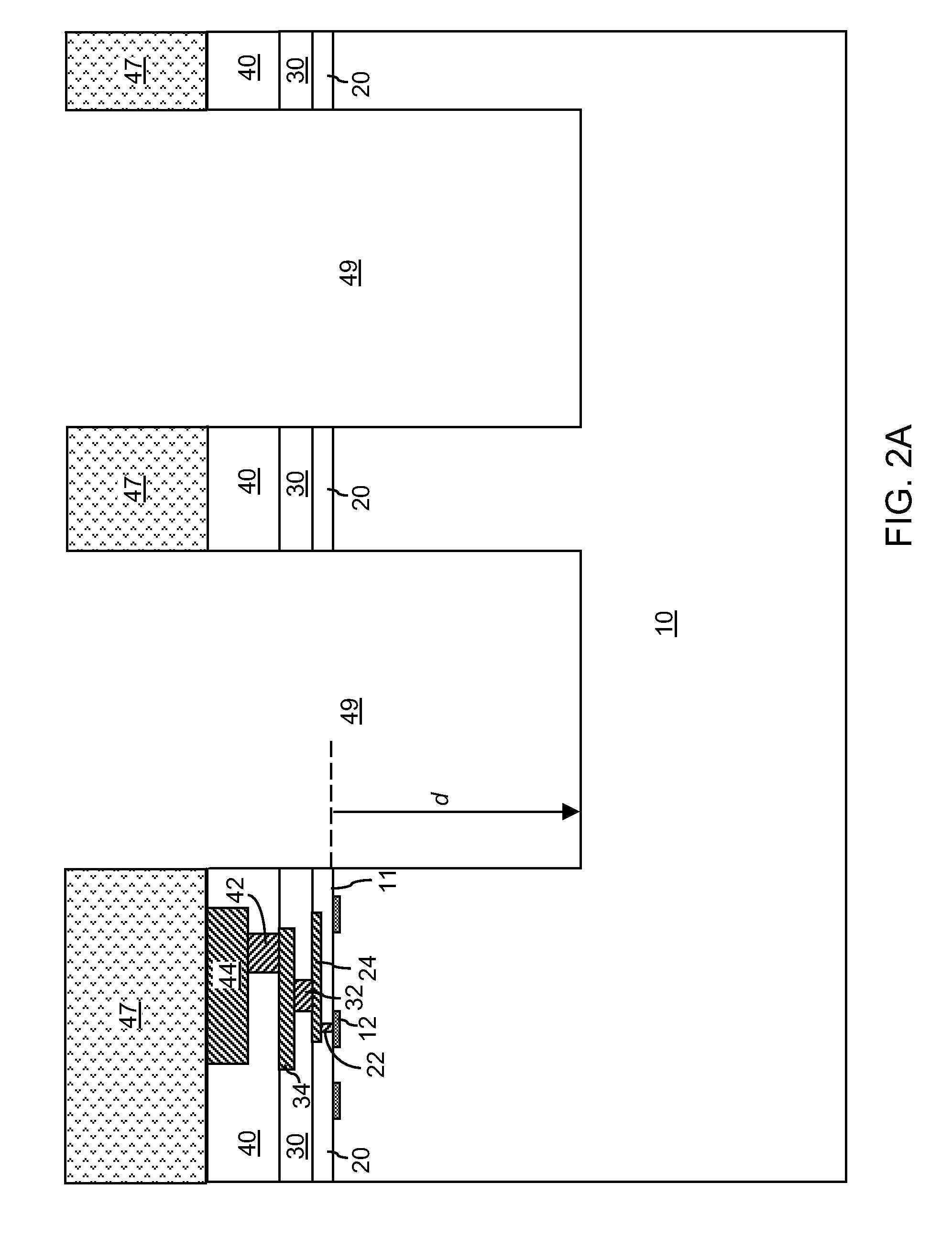
[0025]As stated above, the present disclosure relates to metal-contamination-free through-substrate via structures and methods of manufacturing the same, which are now described in detail with accompanying figures. Throughout the drawings, the same reference numerals or letters are used to designate like or equivalent elements. The drawings are not necessarily drawn to scale.

[0026]As used herein, a “conductive through-substrate via (TSV) structure” is a conductive structure that extends through a substrate, i.e., at least from a top surface of the substrate to a bottom surface of the substrate.

[0027]As used herein, a surface is “substantially planar” if the surface is intended to be planar and the non-planarity of the surface is limited by imperfections inherent in the processing steps that are employed to form the surface.

[0028]As used herein, a “mounting structure” is any structure to which a semiconductor chip can be mounded by making electrical connections thereto. A mounting st...


PUM

PropertyMeasurementUnit
depthaaaaaaaaaa
depthaaaaaaaaaa
radiusaaaaaaaaaa

Abstract

A through-substrate via (TSV) structure that is immune to metal contamination due to a backside planarization process is provided. After forming a through-substrate via (TSV) trench, a diffusion barrier liner is conformally deposited on the sidewalls of the TSV trench. A dielectric liner is formed by depositing a dielectric material on vertical portions of the diffusion barrier liner. A metallic conductive via structure is formed by subsequently filling the TSV trench. Horizontal portions of the diffusion barrier liner are removed. The diffusion barrier liner protects the semiconductor material of the substrate during the backside planarization by blocking residual metallic material originating from the metallic conductive via structure from entering into the semiconductor material of the substrate, thereby protecting the semiconductor devices within the substrate from metallic contamination.

Description

CROSS REFERENCE TO RELATED APPLICATION[0001]This application is a divisional of U.S. patent application Ser. No. 12 / 840,688, filed Jul. 21, 2010, the entire content and disclosure of which is incorporated herein by reference.BACKGROUND[0002]The present disclosure relates to the field of semiconductor structures, and particularly to metal-contamination-free through-substrate via structures and methods of manufacturing the same.[0003]In recent years, “three dimensional silicon” (3DSi) structures have been proposed to enable joining of multiple silicon chips and / or wafers that are mounted on a package or a system board. The 3DSi structures employ conductive via structures, which are referred to as “through-substrate via” structures or “TSV” structures, which provide electrical connection through the substrate of a semiconductor chip. The TSV structures increase the density of active circuits that are integrated in a given space. Such 3DSi structures employ through-substrate vias (TSVs)...

Claims


Application Information

Patent Timeline
Patent Type & Authority Applications(United States)
IPC IPC(8): H01L21/768
CPCH01L21/568H01L21/6835H01L2924/00014H01L2224/16225H01L2924/10253H01L2924/01074H01L2924/01072H01L2924/0105H01L2924/01047H01L2924/01042H01L2924/0104H01L2924/01033H01L2924/01023H01L21/76898H01L23/3171H01L23/481H01L24/03H01L24/05H01L24/06H01L24/11H01L24/13H01L24/16H01L24/81H01L24/93H01L24/94H01L2221/68327H01L2221/6834H01L2221/68381H01L2224/03002H01L2224/0401H01L2224/0557H01L2224/05572H01L2224/05624H01L2224/05647H01L2224/05655H01L2224/06181H01L2224/11002H01L2224/11334H01L2224/131H01L2224/16227H01L2224/81801H01L2224/93H01L2224/94H01L2924/01013H01L2924/01029H01L2924/01032H01L2924/01038H01L2924/01049H01L2924/01073H01L2924/01079H01L2924/12044H01L2924/01006H01L2924/014H01L2224/81H01L2224/03H01L2224/11H01L2924/00H01L2224/05552H01L2924/15788
Inventor FAROOQ, MUKTA G.HANNON, ROBERTVOLANT, RICHARD P.
Owner GLOBALFOUNDRIES U S INC
Why Eureka
Try Eureka