

Method and Structure For Forming ETSOI Capacitors, Diodes, Resistors and Back Gate Contacts
a technology of capacitors and diodes, applied in semiconductor devices, diodes, inductances, etc., can solve problems such as increased leakage current and variability, device dimensions, and recent meeting obstacles
- Summary
- Abstract
- Description
- Claims
- Application Information
AI Technical Summary
Benefits of technology
Problems solved by technology
Method used
Image

Examples
Embodiment Construction
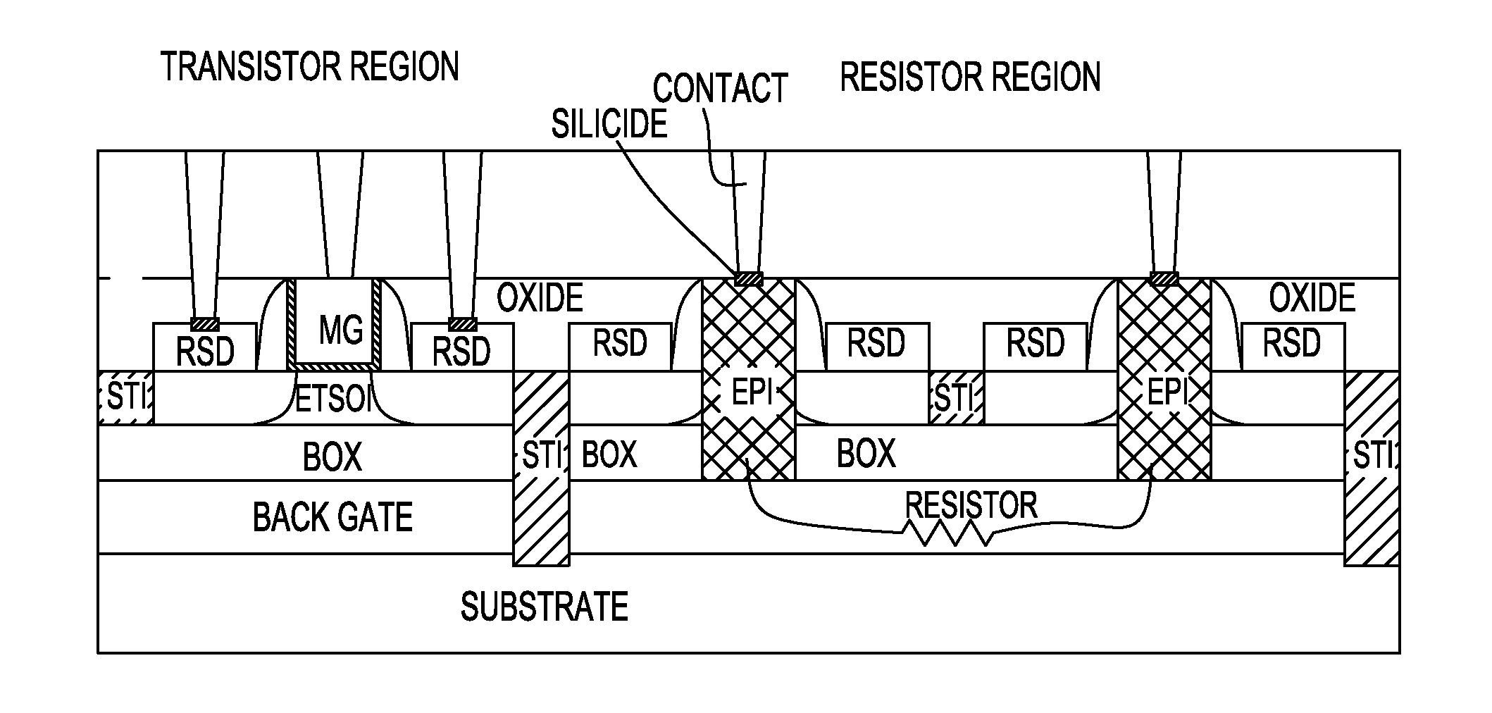
[0027]Detailed embodiments of the present invention are disclosed hereinafter. It is to be understood that they are merely illustrative of the invention that may be embodied in various forms. In addition, each of the examples given in connection with the various aspects of the invention is intended to be illustrative, and not restrictive. Further, the figures are not necessarily drawn to scale, some features may be exaggerated to show details of particular components. Therefore, specific structural and functional details disclosed herein are not to be interpreted as limiting, but merely as a representative basis for teaching one skilled in the art to variously employ the present invention.
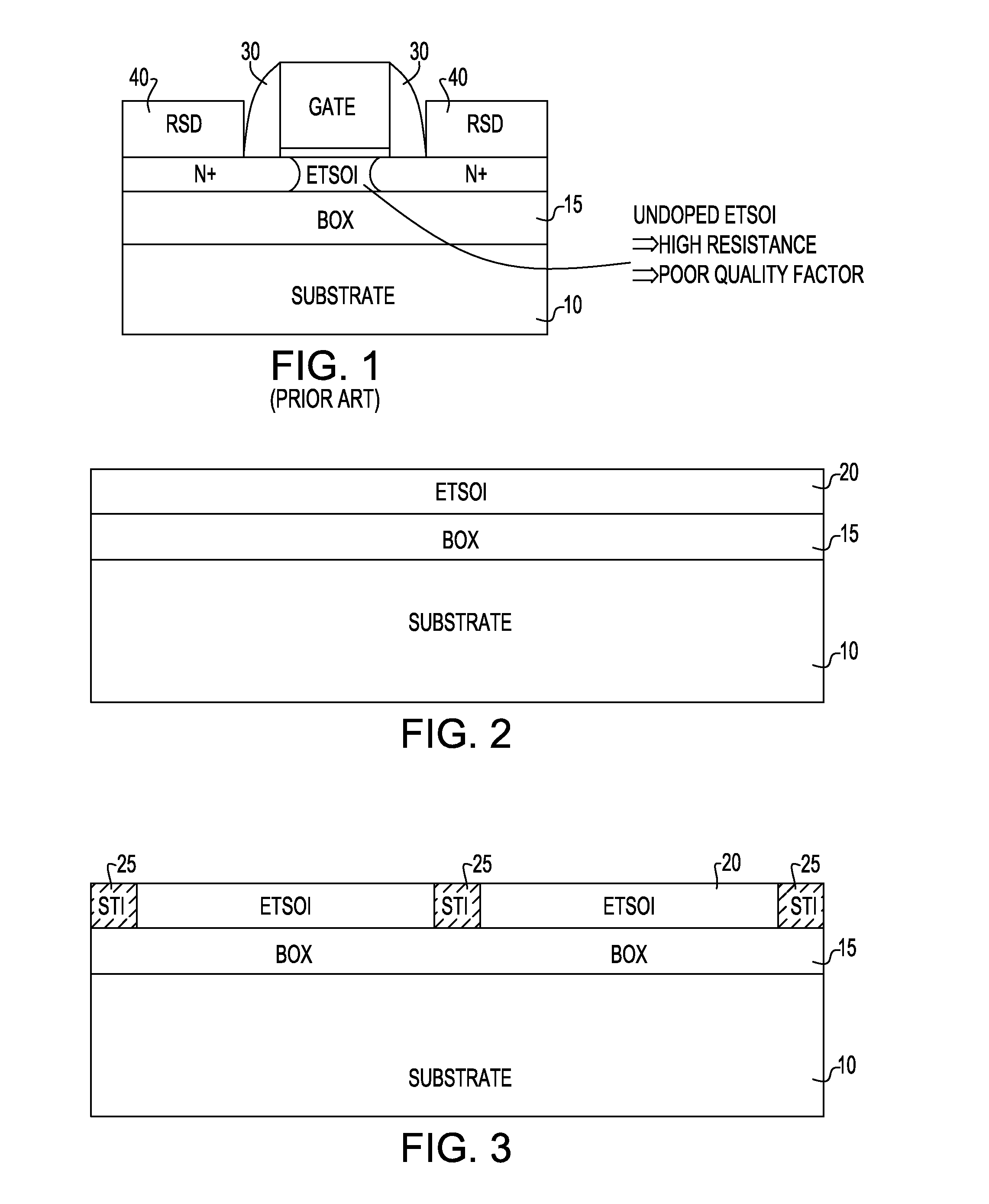
[0028]Referring to FIG. 2, an illustrative structure and a method for forming semiconductor FET devices on a semiconductor-on-insulator (SOI) substrate are described, the structure employing an extremely thin semiconductor-on-insulator (ETSOI) layer 20. The ETSOI layer is deposited directly on top ...
PUM
 Abstract
Description
Claims
Application Information