Eureka AIR delivers breakthrough ideas for toughest innovation challenges, trusted by R&D personnel around the world.

Solar cell and method for manufacturing the same

Active Publication Date: 2013-06-20
SHANGRAO JINKO SOLAR TECH DEV CO LTD
View PDF53 Cites 13 Cited by
  • Summary
  • Abstract
  • Description
  • Claims
  • Application Information

AI Technical Summary

Benefits of technology

The present patent is about a simple method of manufacturing a solar cell with high efficiency. The method involves texturing the surface of a semiconductor substrate with a dopant, forming an emitter layer by ion-doping, and then sequentially adding a back passivation film and electrodes. The resulting solar cell has a surface roughness of about 1 μm or less on its front surface. The technical effects of this invention are to provide a simple method for manufacturing a solar cell with high efficiency and good surface quality.

Problems solved by technology

However, in this case, the manufacturing process is complicated.

Method used


Image

  • Solar cell and method for manufacturing the same
  • Solar cell and method for manufacturing the same
  • Solar cell and method for manufacturing the same

Examples


Embodiment Construction

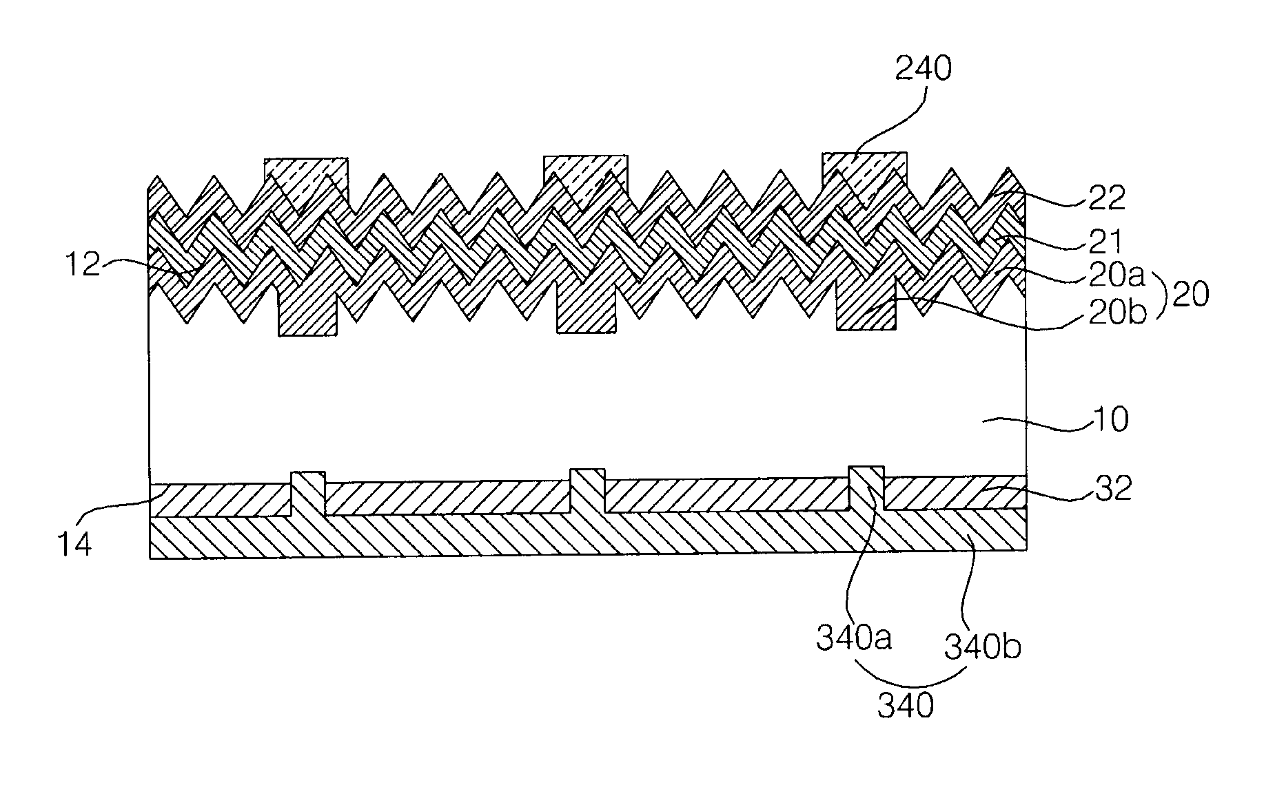
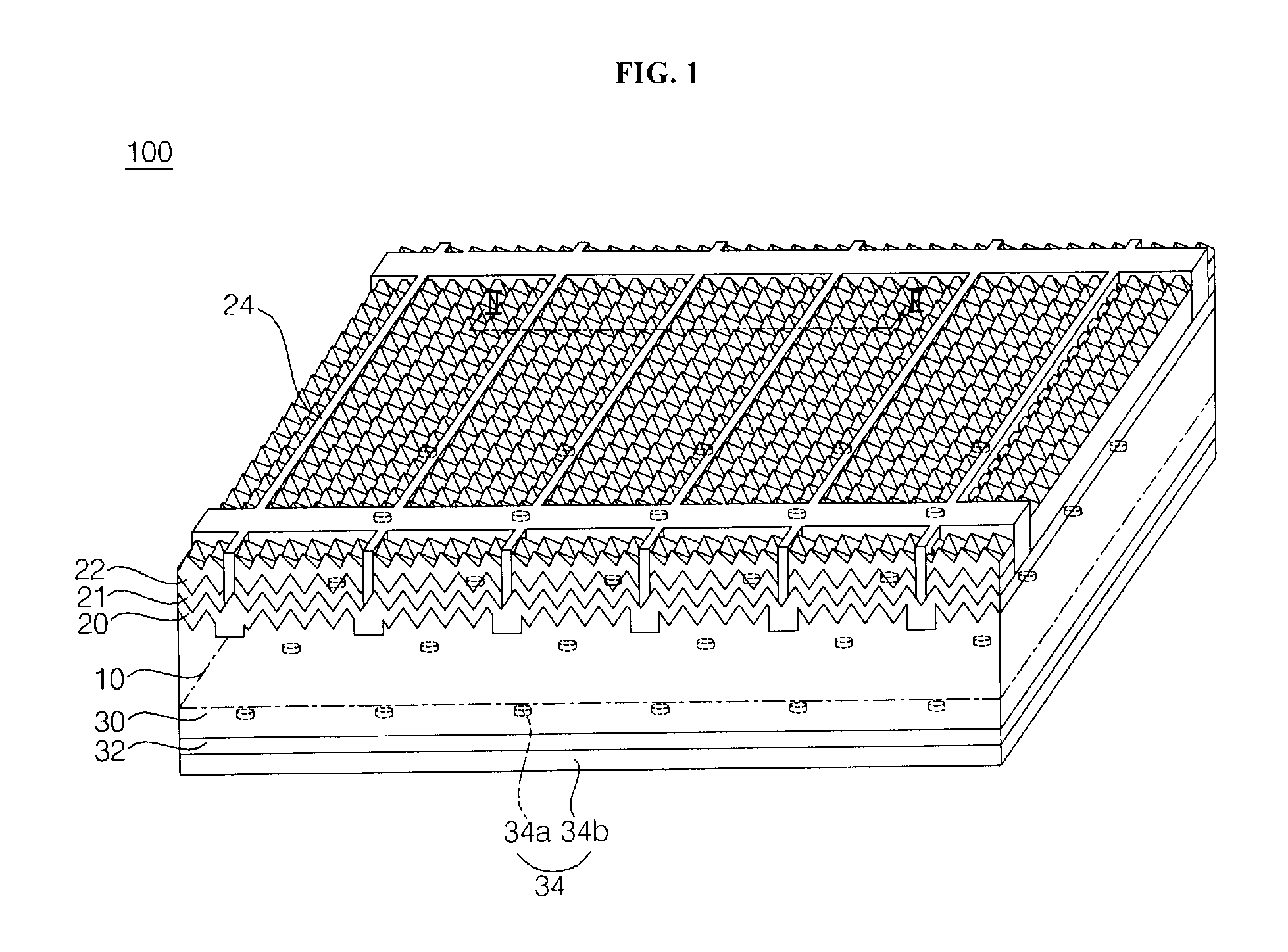
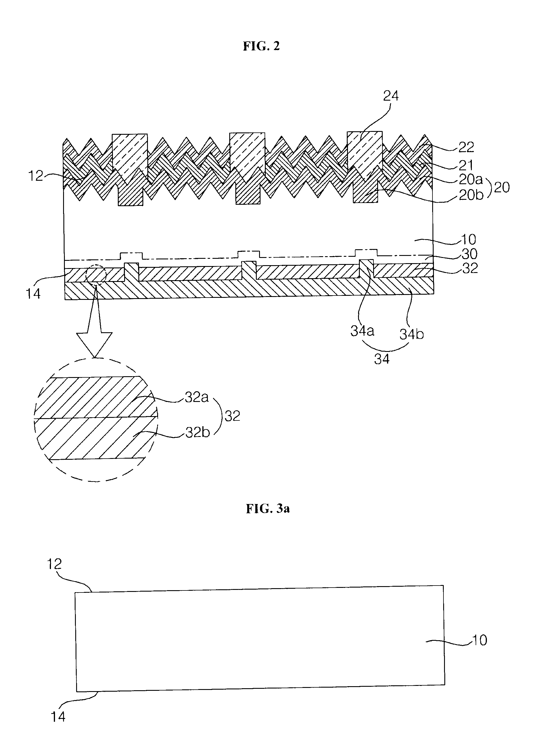
[0013]Hereinafter, embodiments of the present invention will be described with reference to the accompanying drawings. However, the present invention is not limited these embodiments, and various modifications of the exemplary embodiments are possible.

[0014]In order to clearly and concisely illustrate the embodiments, elements not related to the present invention are omitted in the figures. Also, elements similar to or the same as each other have the same reference numerals. In addition, the dimensions of layers and regions are exaggerated or schematically illustrated, or some layers are omitted for clarity of illustration. The dimensions of each part as drawn may not reflect an actual size.

[0015]In the following description, when a layer or substrate “includes” another layer or portion, it can be understood that the layer or substrate further includes still another layer or portion. Also, when a layer or film is referred to as being “on” another layer or substrate, it can be direct...


PUM


Abstract

A method for manufacturing a solar cell includes texturing a front surface of a semiconductor substrate having a first conductive type dopant by using a dry etching method, forming an emitter layer by ion-implanting a second conductive type dopant into the front surface of the semiconductor substrate, forming a back passivation film on a back surface of the semiconductor substrate; and forming a first electrode electrically connected to the emitter layer and a second electrode being in partial contact with the back surface of the semiconductor substrate.

Description

CROSS-REFERENCE TO RELATED APPLICATION[0001]This application claims the priority benefit of Korean Patent Application No. 10-2011-0136467, filed on Dec. 16, 2011, in the Korean Intellectual Property Office, the disclosure of which is incorporated herein by reference.BACKGROUND[0002]1. Field of the Disclosure[0003]The present disclosure relates to a solar cell and a method for manufacturing the same, and more particularly, to a solar cell manufactured by a simple method.[0004]2. Description of the Related Art[0005]In recent times, as it becomes more accepted that conventional energy resource such as petroleum and coal will be exhausted within a foreseeable timeframe, interest in alternative energy sources for replacing the conventional energy resources is gradually increasing. Among the alternative energy sources, a solar cell is spotlighted as a new generation cell using a semiconductor device for directly converting solar energy into electrical energy.[0006]Efficiency improvements ...

Claims


Application Information

Patent Timeline
IPC IPC(8): H01L31/0236H01L31/18
CPCY02E10/547H01L31/068H01L31/02363H01L31/02167H01L31/0216H01L31/0236H01L31/04H01L31/18H01L31/022425H01L31/02366
Inventor LEE, KYOUNGSOOSHIN, MYUNGJUNJEONG, JIWEON
Owner SHANGRAO JINKO SOLAR TECH DEV CO LTD
Why Eureka
Eureka Blog
Learn More