Photoconductive antenna, terahertz wave generating device, camera, imaging device, and measuring device

a terahertz wave and generating device technology, applied in the field of photoconductive antennas, can solve the problems of insufficient intensity of terahertz waves irradiated at the target site, large waste,

Active Publication Date: 2013-06-20
SEIKO EPSON CORP
View PDF3 Cites 7 Cited by
  • Summary
  • Abstract
  • Description
  • Claims
  • Application Information

AI Technical Summary

Benefits of technology

[0035]With this configuration, it is possible to provide a camera having the effects of the invention.
[0036]An imaging device according to another aspect of the present invention includes the photoconductive antenna according to the above mentioned aspects, a light source configured and arranged to generate the pulsed light, a terahertz wave detecting unit configured and arranged to detect the terahertz waves emitted from the photoconductive antenna and transmitted through an object or reflected by the object, and an image forming unit configured and arranged to generate an image of the object based on detection results of the terahertz wave detecting unit.
[0037]With this configuration, it is possible to provide an imaging device having the effects of the present invention.
[0038]A measuring device according to another aspect of the present invention includes the photoconductive antenna according to the above mentioned aspects, a light source configured and arranged to generate the pulsed light, a terahertz wave detecting unit configured and arranged to detect the terahertz waves emitted from the photoconductive antenna and transmitted through an object or reflected by the object, and a measuring unit configured and arranged to measure the object based on detection results of the terahertz wave detecting unit.
[0039]With this configuration, it is possible to provide a measuring device having the effects of the present invention.

Problems solved by technology

However, with the photoconductive antenna noted in Japanese Laid-Open Patent Application Publication No. 2007-300022, terahertz waves with no directionality are generated, so there is a great deal of waste, and the intensity of the terahertz waves irradiated at the target site was insufficient.

Method used


Image

  • Photoconductive antenna, terahertz wave generating device, camera, imaging device, and measuring device
  • Photoconductive antenna, terahertz wave generating device, camera, imaging device, and measuring device
  • Photoconductive antenna, terahertz wave generating device, camera, imaging device, and measuring device

Examples


first embodiment

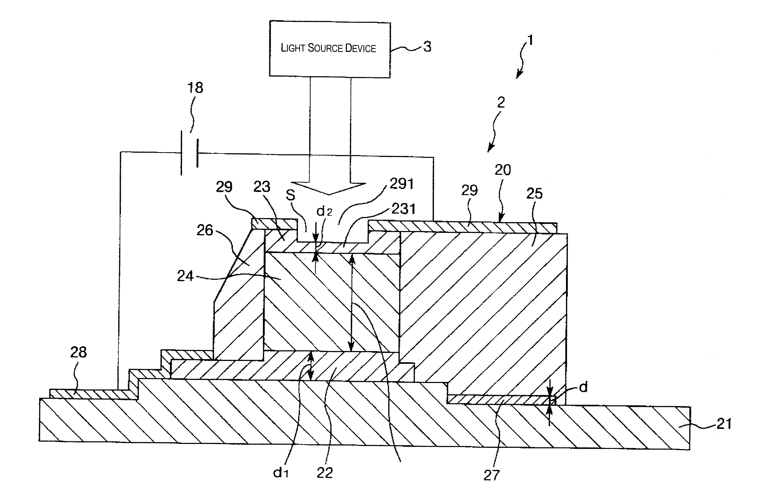
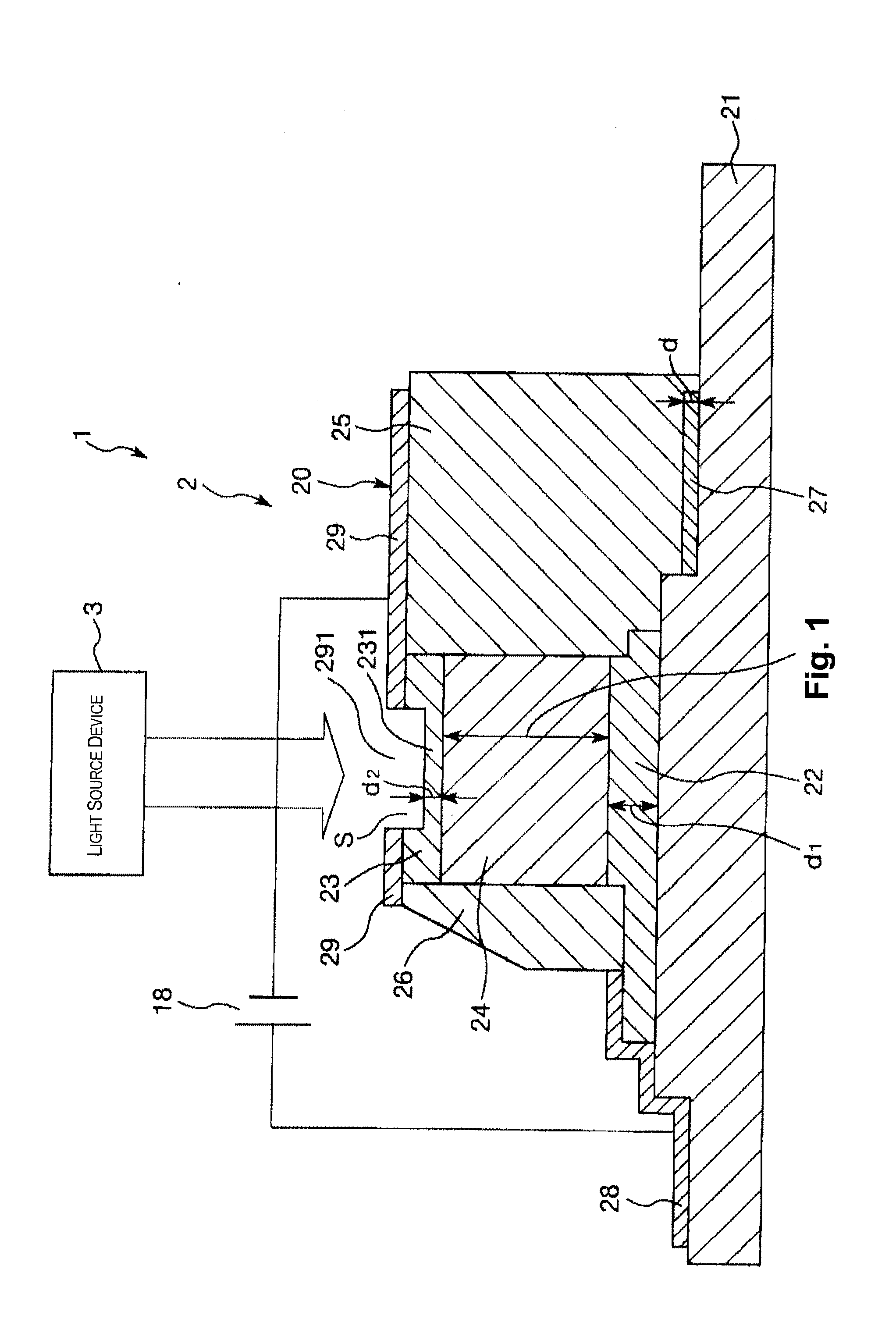
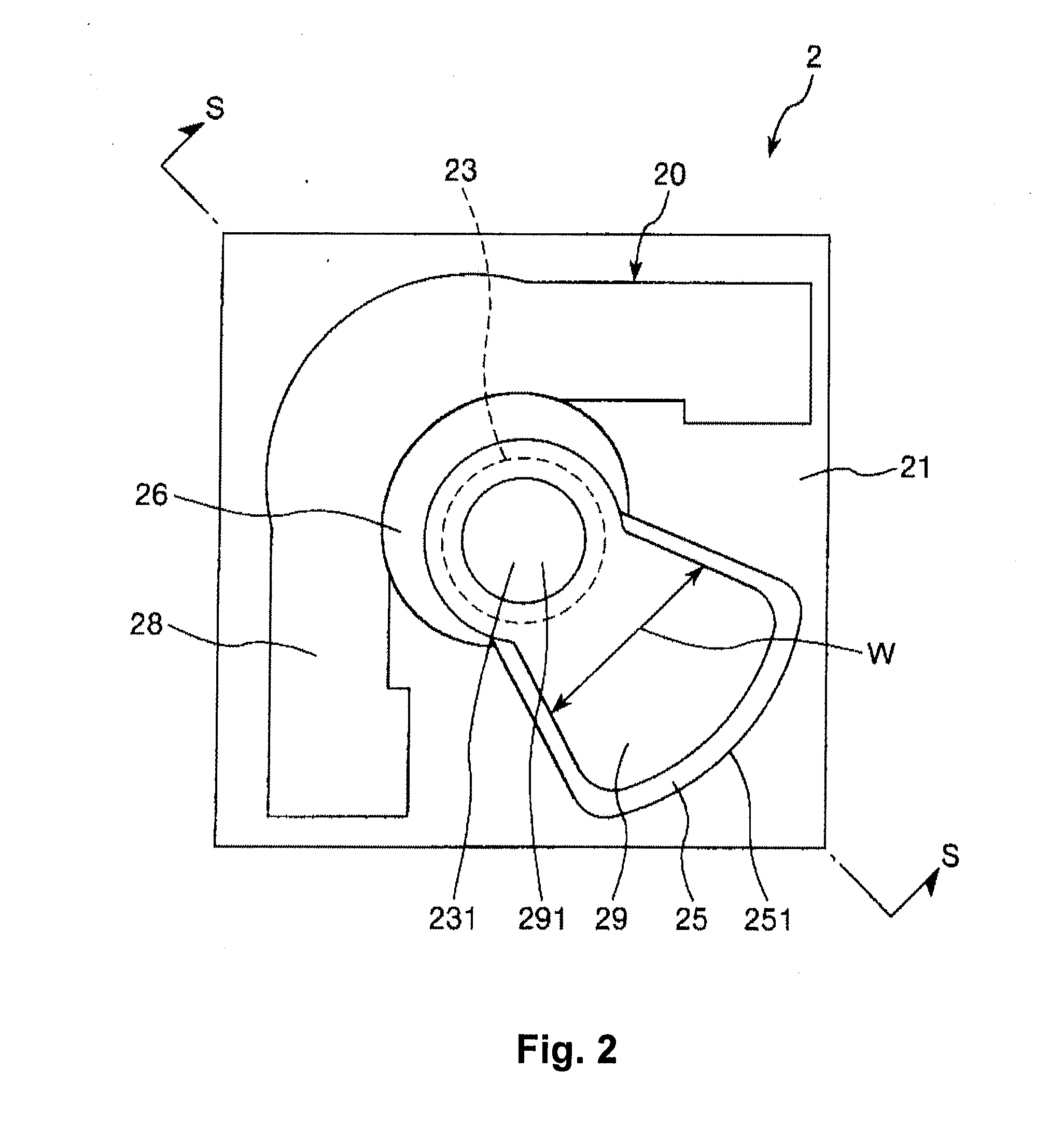
[0054]FIG. 1 is a drawing showing an embodiment of the terahertz wave generating device of the present invention. With this FIG. 1, a cross section view of line S-S in FIG. 2 is shown for the photoconductive antenna, and a block diagram is shown for the light source device. FIG. 2 is a plan view of the photoconductive antenna of the terahertz wave generating device shown in FIG. 1. FIG. 3 is a cross section perspective view of the light source device of the terahertz wave generating device shown in FIG. 1. FIG. 4 is a cross section view of line A-A in FIG. 3. FIG. 5 is a cross section view of line B-B in FIG. 3. Note that hereafter, in FIG. 1 and FIG. 3 to FIG. 5, the upper side will be described as “upper” and the lower side will be described as “lower.”

[0055]As shown in FIG. 1, the terahertz wave generating device 1 has a light source device 3 that generates light pulses (pulsed light) which is excitation light, and a photoconductive antenna 2 for generating terahertz waves by irr...

embodiment

of Camera

[0139]FIG. 11 is a block diagram showing the embodiment of the camera of the present invention. Also, FIG. 12 shows a schematic perspective view showing an embodiment of the camera of the present invention.

[0140]Following, the description of the embodiment of the camera will focus on the differences from the previously described embodiment of the image device, the same items are given the same code numbers as in the previously described embodiments, and a detailed description of those will be omitted.

[0141]As shown in FIG. 11 and FIG. 12, the camera 300 is equipped with a terahertz wave generating unit 9 for generating terahertz waves, a terahertz wave detecting unit 11 for detecting terahertz waves emitted from the terahertz wave generating unit 9 and reflected by the object 170, and a memory unit 14. Then, each of these parts is housed in a case 310 of the camera 300. Also, the camera 300 is equipped with a lens (optical system) 320 for converging (imaging) the terahertz ...


PUM


Abstract

A photoconductive antenna is adapted to generate terahertz waves when irradiated by pulsed light. The photoconductive antenna includes first and second conductive layers, a semiconductor layer positioned between the first and second conductive layers, first and second electrodes, and a dielectric layer. The semiconductor layer is made of a semiconductor material having a carrier density that is lower than a carrier density of the semiconductor material of the first conductive layer or the second conducive layer. The first and second electrodes are electrically connected to the first and second conductive layers, respectively. The second electrode has an aperture through which the pulsed light passes. The dielectric layer is made of a dielectric material, and is in contact with a surface of the semiconductor layer having a normal direction extending orthogonal to a lamination direction of the first conductive layer, the semiconductor layer, and the second conductive layer.

Description

CROSS-REFERENCE TO RELATED APPLICATIONS[0001]This application claims priority to Japanese Patent Application No. 2011-278883 filed on Dec. 20, 2011. The entire disclosure of Japanese Patent Application No. 2011-278883 is hereby incorporated herein by reference.BACKGROUND[0002]1. Technical Field[0003]The present invention relates to a photoconductive antenna, a terahertz wave generating device, a camera, an imaging device, and a measuring device.[0004]2. Related Art[0005]In recent years, attention has been devoted to terahertz waves, which are electromagnetic waves with frequencies of 100 GHz or greater and 30 THz or less. Terahertz waves can be used in various forms of measurement and non-destructive testing such as imaging and spectrometry.[0006]The terahertz wave generating device that generates these terahertz waves has a light source device that generates light pulses (pulsed light) having pulse widths at the approximately sub picosecond level (several hundred femtoseconds) and ...

Claims


Application Information

Patent Timeline
Patent Type & Authority Applications(United States)
IPC IPC(8): H01L33/00H01L31/16G01S17/89
CPCH01L31/16H01L33/0004H01L31/09G01N21/3581H01L27/14625G01S17/89G01S13/89H01L27/14603H01L27/1446
Inventor TOMIOKA, HIROTO
Owner SEIKO EPSON CORP
Why Eureka
Try Eureka