Pixellated detector device

a detector device and pixel technology, applied in the field of pixel detectors, can solve the problems of increasing undesirable light crosstalk, detector exactly misses the most of the area of the crystal where the highest light output occurs, and serious impediments to adopting this new technology, so as to reduce the optical crosstalk between pixels and achieve the effect of higher light collection efficiency and reduced optical crosstalk

Active Publication Date: 2013-06-20
KONINKLIJKE PHILIPS ELECTRONICS NV
View PDF17 Cites 18 Cited by
  • Summary
  • Abstract
  • Description
  • Claims
  • Application Information

AI Technical Summary

Benefits of technology

[0009]It is an object of the present invention to provide a pixellated detector device with reduced optical crosstalk between pixels, and with higher light collection efficiency.

Problems solved by technology

A timing resolution significantly better than one nanosecond is becoming more valuable as time-of-flight PET (TOF-PET) scanners are becoming more prevalent, however, there have been serious impediments to adopting this new technology.
In a typical one-to-one coupling, however, the sensitive area of each detector pixel is centered below one scintillator crystal, while the non-sensitive areas of the chip (readout electronics etc.) are placed below the ‘gaps’ between the crystals which means that such a detector exactly misses most of the area of the crystal where the highest light output occurs.
In addition, light from these ‘gaps’ can instead reach neighboring detector pixels, thereby increasing the undesirable light crosstalk.
Structuring the glass plate might be a solution but is risky and expensive.
Consequently, in the above conventional technical approach based on a one-to-one coupling of scintillator pixels and detector pixels (e.g. SiPM pixels) signal is lost, and it is extremely difficult to avoid optical crosstalk between pixels.

Method used


Image

  • Pixellated detector device
  • Pixellated detector device
  • Pixellated detector device

Examples


first embodiment

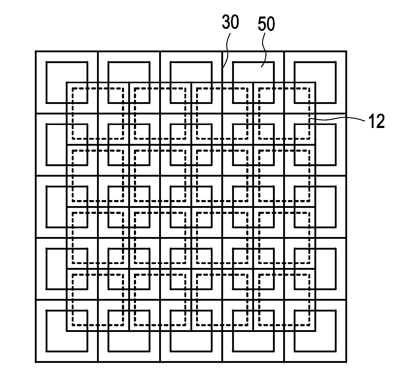
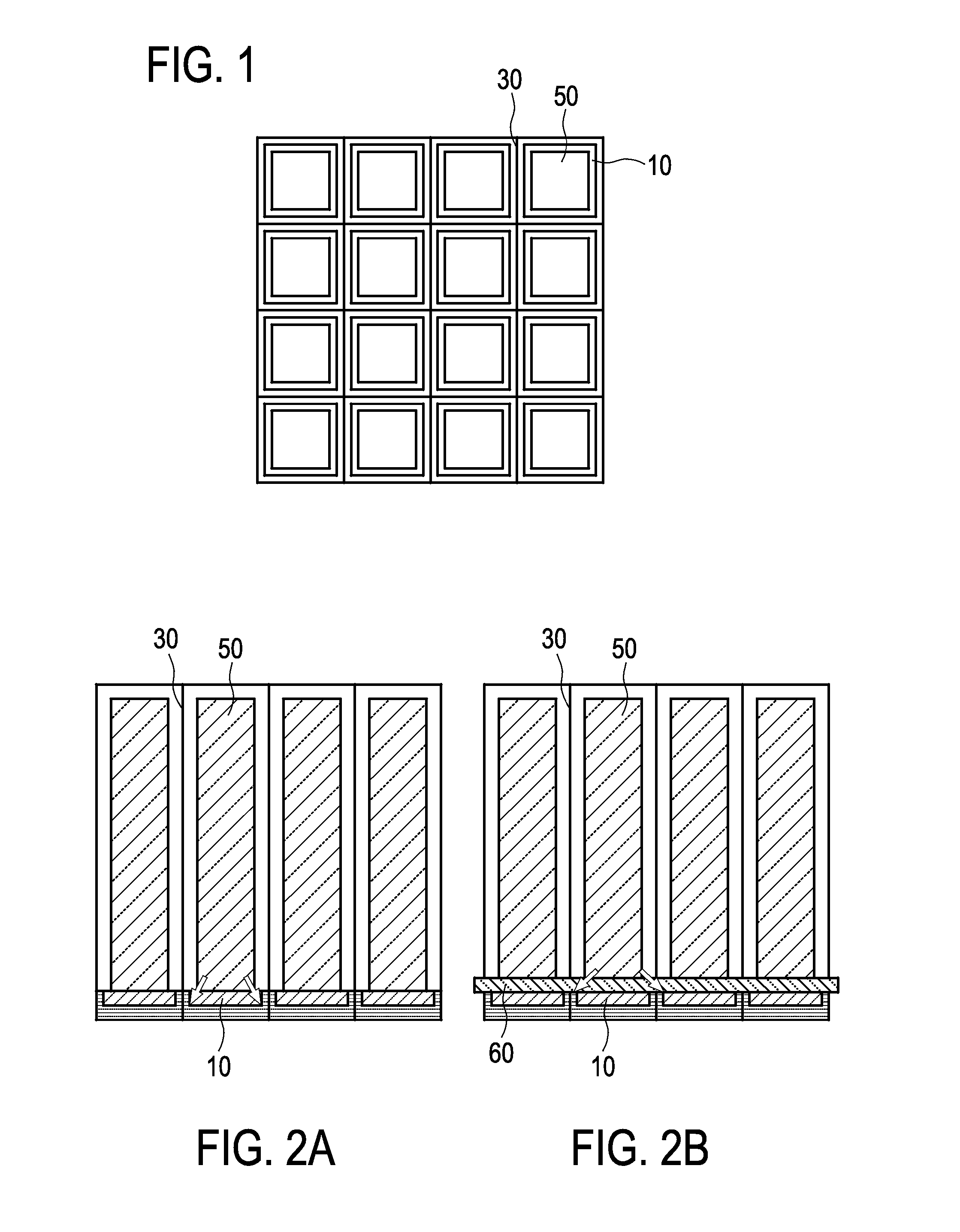
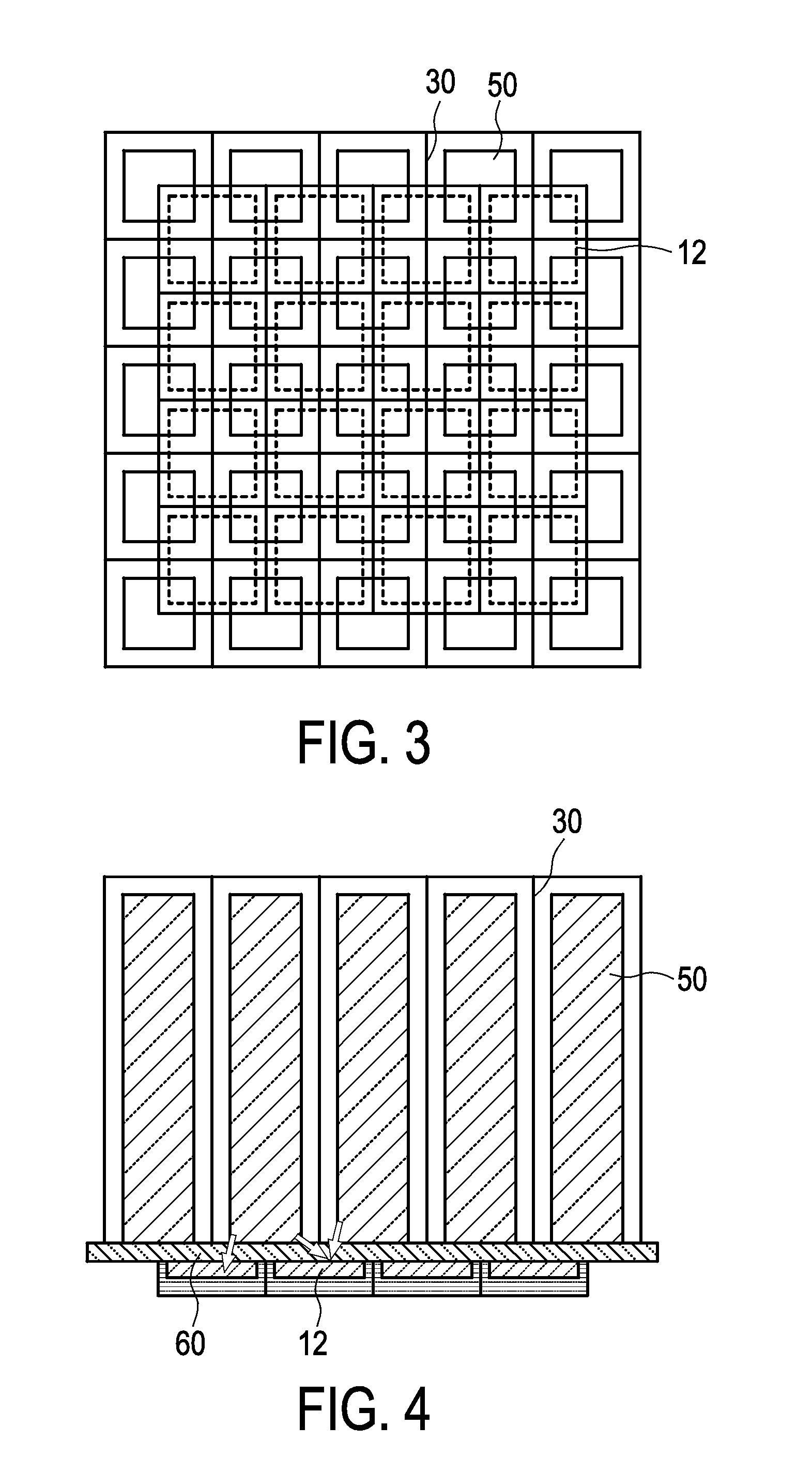
[0032]FIG. 3 shows a top view of a pixellated detector device according to a A half-pixel shift is introduced between scintillator crystals 50 (with their reflective layer 30) and detector pixels 12 and enables the identification of a scintillator crystal 50 from four detector pixels 12 instead of nine pixels in case of optical crosstalk. Glass plates without any mechanical structuring may be used as a common substrate 60 (not shown in FIG. 3) for detector pixels 12 with the photosensitive areas 12 of the detector array and scintillator crystals 50 of the crystal array. Mounting accuracy and costs are strongly reduced. Even a different pixel and crystal pitch can be used, enabling an exact crystal pitch with tiled detectors.

[0033]FIG. 4 shows a cross-section of the pixellated detector device according to the first embodiment with the common substrate 60 and the reflective layer 30. As indicated by the arrows in FIG. 4, light emitted at crystal edges of two neighboring scintillator ...

second embodiment

[0038]FIG. 5 shows a top view of a pixellated detector device with a brick-type pixel structure, a reflective layer 30 and scintillator crystals 50. This modification provides a sort of brick structure where two neighboring detector pixels 70 are merged, either by chip design or by software binning This enables crystal identification from only three detector pixels with doubled pixel area. The dark count rate will be increased by 50% but the data readout rate from the detector array (e.g. SiPM chip) will be halved. In view of the maximum readout rates from a complete PET system this might be a cost saving solution.

[0039]FIG. 6 shows a top view of a pixellated detector device according to a third embodiment with a larger pixel area, a reflective layer 30 and scintillator crystals 50. This modification uses four times larger detector pixels 72 than the first embodiment, with one scintillator crystal 50 centered above the detector pixel 72 and neighboring crystals centered above two o...


PUM


Abstract

The present invention relates to a pixellated detector with an enhanced structure to enable easy pixel identification even with high light output at crystal edges. A half-pixel shift between scintillator crystals (50) and detector pixels (12) enables the identification of a crystal (50) from four detector pixels (12) instead of nine pixels in case of optical crosstalk. Glass plates without any mechanical structuring may be used as a common substrate (60) for detectors and scintillators.

Description

FIELD OF THE INVENTION[0001]The present invention relates to a pixellated detector device for use in nuclear imaging, such as positron emission tomography (PET). More specifically, the present invention relates to a pixellated detector in which an array of scintillator material is coupled to an array of photodetectors, such as in PET or in single photon emission computed tomography (SPECT).BACKGROUND OF THE INVENTION[0002]In past nuclear imaging devices, gamma radiation detectors employ scintillators that convert incident gamma radiation into light, which is then detected by photomultiplier tubes (PMTs). A scintillator is a material which exhibits scintillation - the property of luminescence when excited by ionizing radiation. Due to several drawbacks of photomultiplier tubes, there is interest in replacing them with solid state light sensors, such as avalanche photodiodes driven in Geiger mode, called e.g., silicon photomultipliers (SiPMs). Typical SiPMs have better timing and ener...

Claims


Application Information

Patent Timeline
Patent Type & Authority Applications(United States)
IPC IPC(8): G01T1/20H01L31/18
CPCG01T1/2018G01T1/249H01L27/14663G01T1/2006H01L31/18G01T1/208G01T1/20183G01T1/20187G01T1/20184G01T1/20182
Inventor WIECZOREK, HERFRIED KARLTHON, ANDREAS
Owner KONINKLIJKE PHILIPS ELECTRONICS NV
Why Eureka
Try Eureka