Storage device

a storage device and structure technology, applied in the direction of information storage, static storage, digital storage, etc., can solve the problems of large noise and large differences, and achieve the effects of reducing noise, data storage capacity, and reducing the minimum feature siz

Inactive Publication Date: 2013-06-20
SEMICON ENERGY LAB CO LTD
View PDF3 Cites 54 Cited by
  • Summary
  • Abstract
  • Description
  • Claims
  • Application Information

AI Technical Summary

Benefits of technology

[0019]One embodiment of the present invention enables a reduction of noise attributed to a signal of a word line, in a first bit line and a second bit line which are overlapped with the same word line, in the case where memory cells are stacked in a three-di

Problems solved by technology

However, stacking memory cells simply in a three-dimensional manner leads to a large difference of noise attributed to the signal of the word line, between the first bit line and the second bit lin

Method used


Image

  • Storage device
  • Storage device
  • Storage device

Examples


embodiment 1

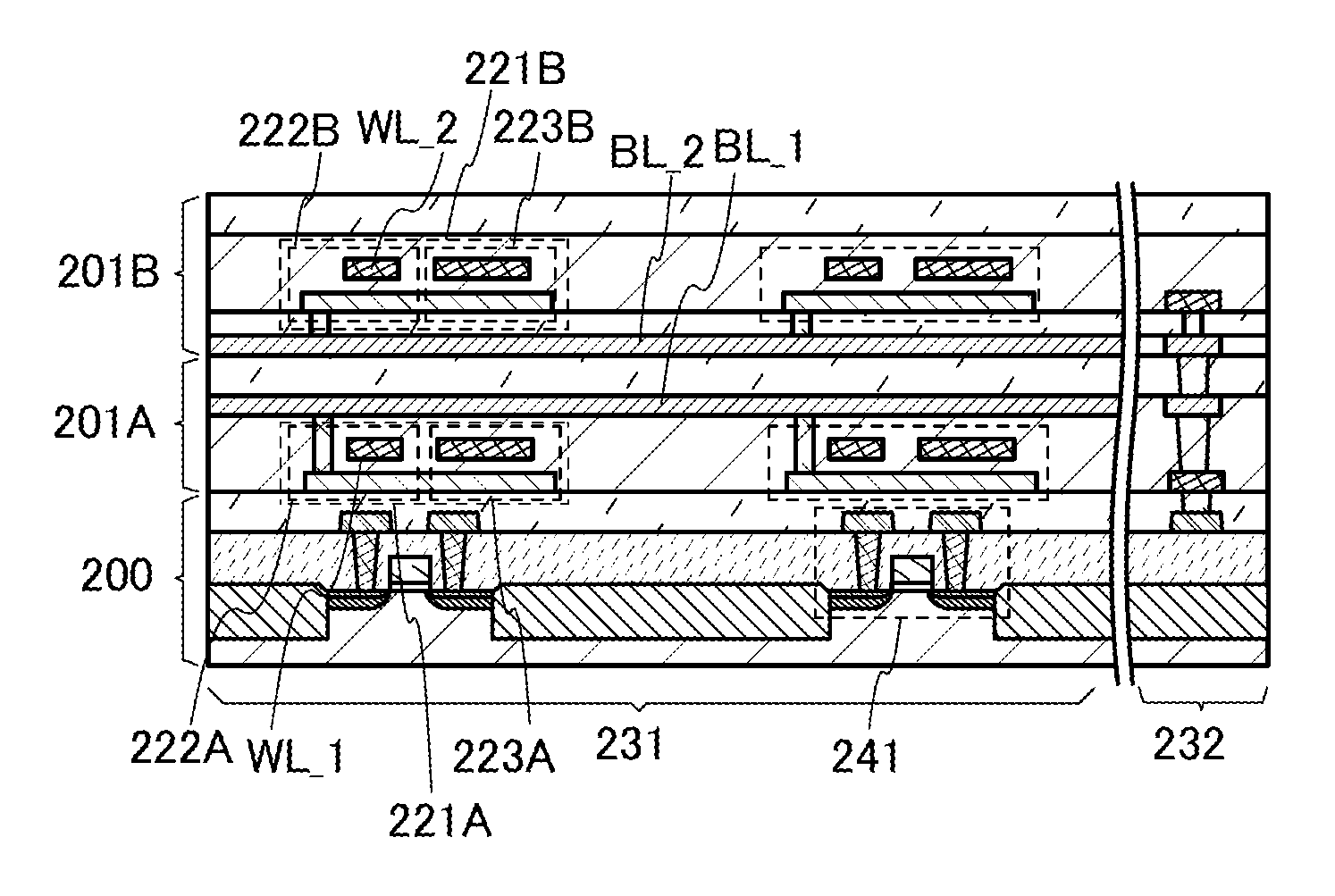
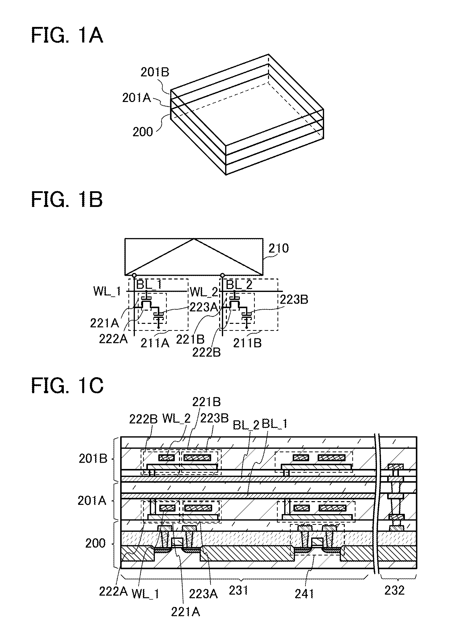
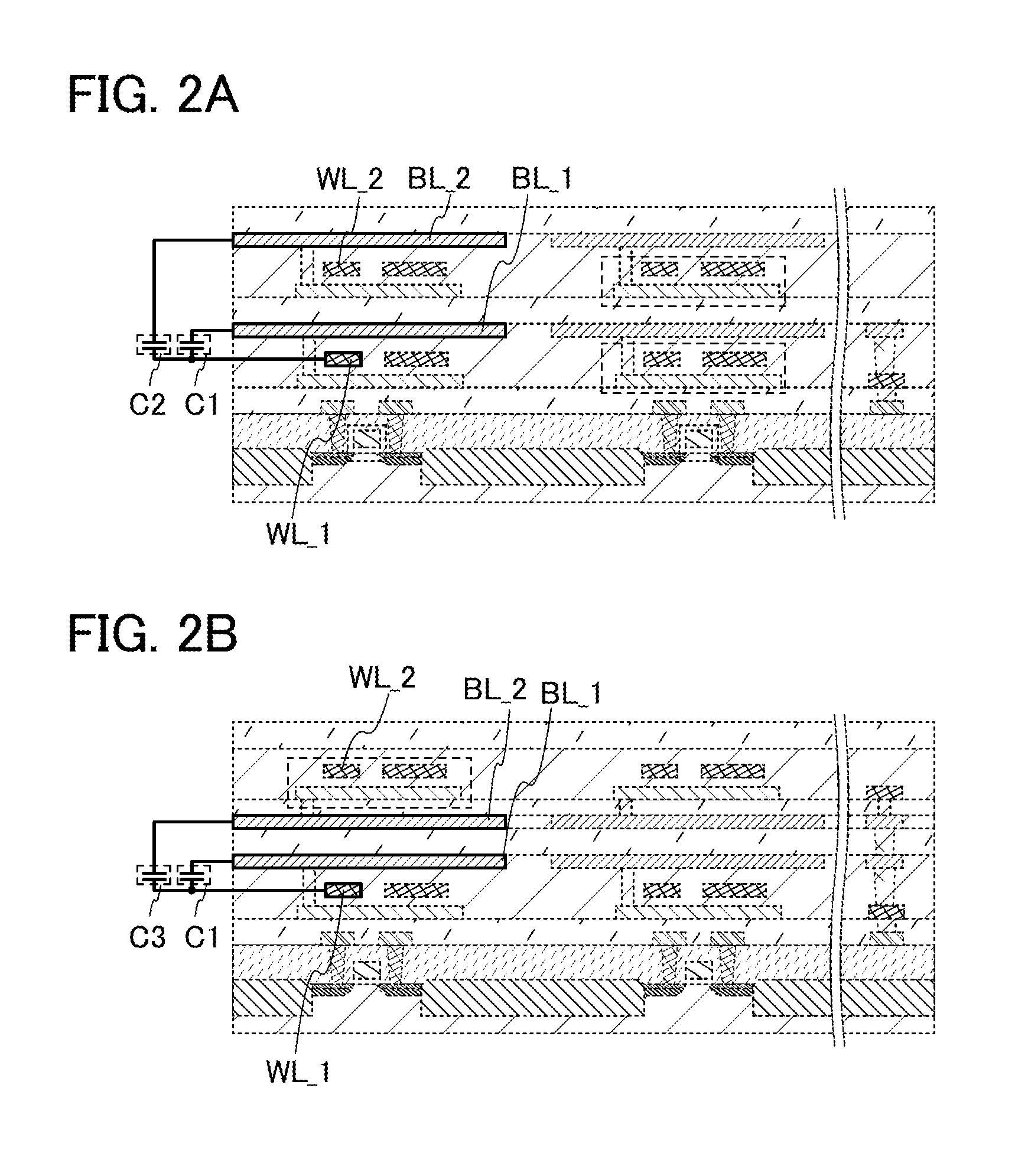
[0040]A structure of a storage device of one embodiment of the present invention is described with reference to FIGS. 1A to 1C, FIGS. 2A and 2B, FIGS. 3A and 3B, FIG. 4, FIG. 5, and FIG. 6.

[0041]FIG. 1A is a conceptual diagram illustrating one example of a structure of a storage device. A storage device of one embodiment of the present invention has a stacked-layer structure in which a plurality of memory cell arrays is provided in an upper portion, and a driver circuit for driving the plurality of memory cell arrays is provided in a lower portion. The driver circuit may include a control circuit, a logic circuit, or an analog circuit. The driver circuit may also include an arithmetic circuit.

[0042]A storage device shown in FIG. 1A includes a memory cell array 201A (also called first memory cell array) including a plurality of memory cells and a memory cell array 201B (also called second memory cell array) including a plurality of memory cells in its upper portion, and includes a dr...

embodiment 2

[0098]In this embodiment, a structure and a manufacturing method of a storage device of one embodiment of the present invention are described with reference to FIGS. 7A and 7B, FIG. 8, FIGS. 9A and 9B, and FIGS. 10A and 10B.

[0099]FIG. 7A is a cross-sectional diagram of a storage device. FIG. 7A is the cross-sectional diagram parallel to the channel length direction of a transistor in the storage device. The storage device illustrated in FIG. 7A includes the memory cell array 201A and the memory cell array 201B in its upper portion and the driver circuit 200 in its lower portion. Further, the first memory cell 221A is illustrated as a typical example in the memory cell array 201A, and the second memory cell 221B is illustrated as a typical example in the memory cell array 201B.

[0100]FIG. 7B illustrates a structure of the memory cell 221A in FIG. 7A in detail. The memory cell 221B provided over the memory cell 221A can have a structure which is similar to that of the memory cell 221A ...

embodiment 3

[0184]In this embodiment, application of the storage device described in any of the above embodiments to a semiconductor device such as an electronic device is described with reference to FIGS. 12A to 12F. In this embodiment, application of the above-described storage device to electronic devices such as a computer, a cellular phone (also referred to as a mobile phone or a mobile phone set), a portable information terminal (including a portable game machine, an audio reproducing device, and the like), a camera such as a digital camera or a digital video camera, electronic paper, and a television set (also referred to as a television or a television receiver) is described.

[0185]FIG. 12A illustrates a laptop personal computer including a housing 701, a housing 702, a display portion 703, a keyboard 704, and the like. At least one of the housings 701 and 702 is provided with the storage device described in any of the above embodiments is provided. Accordingly, a laptop personal compute...


PUM


Abstract

Noise attributed to signals of a word line, in first and second bit lines which are overlapped with the same word line in memory cells stacked in a three-dimensional manner is reduced in a storage device with a folded bit-line architecture. The storage device includes a driver circuit including a sense amplifier, and first and second memory cell arrays which are stacked each other. The first memory cell array includes a first memory cell electrically connected to the first bit line and a first word line, and the second memory cell array includes a second memory cell electrically connected to the second bit line and a second word line. The first and second bit lines are electrically connected to the sense amplifier in the folded bit-line architecture. The first word line, first bit line, second bit line, and second word line are disposed in this manner over the driver circuit.

Description

BACKGROUND OF THE INVENTION[0001]1. Field of the Invention[0002]The present invention relates to a structure of a storage device. In particular, the present invention relates to a structure of a folded dynamic RAM (dynamic random access memory: DRAM).[0003]2. Description of the Related Art[0004]The cost for a DRAM that is a storage device has been lowering; to further lower the cost, an increase in capacity has been actively researched and developed. The increase in capacity can be achieved by, for example, changing the layout of the memory cell and miniaturizing the element, but such a scale down of the dimension of the memory cell or reduction in the size of the element is limited.[0005]In terms of the layout change of a memory cell, either an open bit-line architecture or a folded bit-line architecture may be adopted. The open bit-line architecture enables a scale down of the dimension of the memory cell but is weak against noise at the time of data reading. On the other hand, th...

Claims


Application Information

Patent Timeline
IPC IPC(8): G11C7/06
CPCG11C7/06G11C11/4097G11C11/4091G11C5/02
Inventor ATSUMI, TOMOAKI
Owner SEMICON ENERGY LAB CO LTD
Why Eureka
Try Eureka