Multilayer ceramic electronic component and fabrication method thereof

a multi-layer ceramic and electronic component technology, applied in the direction of variable capacitors, fixed capacitor details, fixed capacitors, etc., can solve the problems of failure to ensure reliability and difficulty in reducing the size of multi-layer ceramic elements, and achieve excellent reliability, high capacitance, and the effect of reducing thickness deviations

Active Publication Date: 2013-07-18
SAMSUNG ELECTRO MECHANICS CO LTD
View PDF3 Cites 23 Cited by
  • Summary
  • Abstract
  • Description
  • Claims
  • Application Information

AI Technical Summary

Benefits of technology

[0010]An aspect of the present invention provides a high capacitance multilayer ceramic electronic component having excellent reliability, while having thinner external electrodes, by reducing thickness deviations in the external electrodes.

Problems solved by technology

In addition, since external electrodes have also been required to become thinner, potentially causing a defect in which a plating solution infiltrates into a chip therethrough, it is difficult to reduce the size of the multilayered ceramic element.
In particular, when the shape of the external electrodes is not uniform, the possibility of the plating solution infiltrating a thinner portion thereof is further increased, resulting in a failure to secure reliability.

Method used


Image

  • Multilayer ceramic electronic component and fabrication method thereof
  • Multilayer ceramic electronic component and fabrication method thereof
  • Multilayer ceramic electronic component and fabrication method thereof

Examples


first embodiment

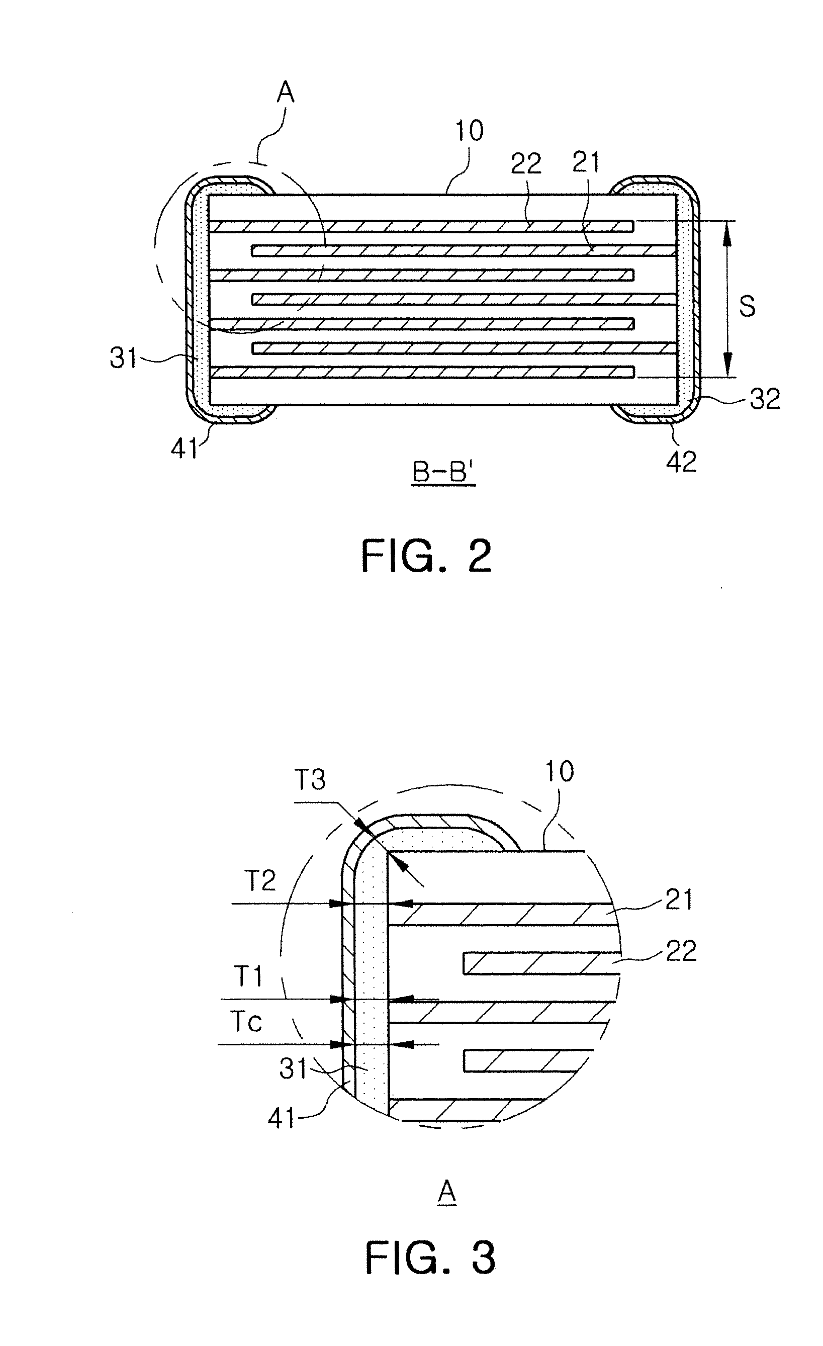
[0038]FIG. 3 is an enlarged view of portion ‘A’ in FIG. 2 according to the present invention.

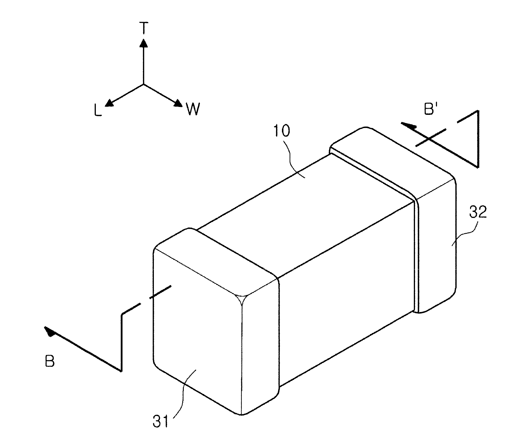
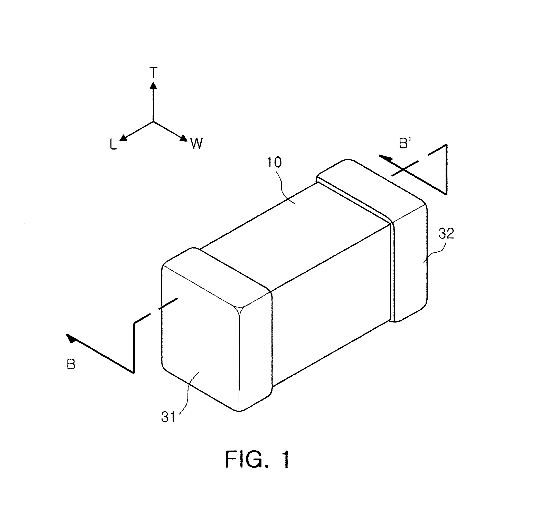
[0039]With reference to FIGS. 1 through 3, a multilayer ceramic electronic component according to the first embodiment of the present invention may include: a ceramic main body 10; a plurality of internal electrodes 21 and 22 laminated within the ceramic main body; and external electrodes 31 and 32 formed on outer surfaces of the ceramic main body 10 and electrically connected to the internal electrodes 21 and 22, wherein an average thickness of the external electrodes 31 and 32 is 10 μm or less, and when a thickness of the external electrodes 31 and 32 at a central portion of the ceramic main body 10 in a thickness direction is Tc and a thickness of the external electrodes 31 and 32 spaced apart from a central portion of a capacitance formation region in a thickness direction in which the internal electrodes 21 and 22 are laminated to contribute to capacitance formation by a distance equal ...

second embodiment

[0077]FIG. 4 is an enlarged view of portion ‘A’ in FIG. 2 according to the present invention.

[0078]With reference to FIG. 4, the multilayer ceramic electronic component according to the second embodiment of the present invention may include: a ceramic main body 10; a plurality of internal electrodes 21 and 22 laminated within the ceramic main body 10; and external electrodes 31 and 32 formed on outer surfaces of the ceramic main body 10 and electrically connected to the internal electrodes 21 and 22, wherein an average thickness of the external electrodes 31 and 32 is 10 μm or less, and when a thickness of the external electrodes 31 and 32 at a central portion of the ceramic main body 10 in a thickness direction is Tc and a thickness of the external electrodes 31 and 32 at an outermost internal electrode of the ceramic main body 10 in which the internal electrodes 21 and 22 are laminated to contribute to capacitance formation is T2, 0.5≦|T2 / Tc|≦1.0 may be satisfied.

[0079]When a thin...

third embodiment

[0087]FIG. 5 is an enlarged view of portion ‘A’ in FIG. 2 according to the present invention.

[0088]With reference to FIG. 5, the multilayer ceramic electronic component according to the third embodiment of the present invention may include: a ceramic main body 10; a plurality of internal electrodes 21 and 22 laminated within the ceramic main body 10; and external electrodes 31 and 32 formed on outer surfaces of the ceramic main body 10 and electrically connected to the internal electrodes 21 and 22, wherein an average thickness of the external electrodes 31 and 32 is 10 μm or less, and when a thickness of the external electrodes 31 and 32 at a central portion of the ceramic main body 10 in a thickness direction is Tc, a thickness of the external electrodes 31 and 32 at a point spaced apart from a central portion of a capacitance formation region in the thickness direction in which the internal electrodes are laminated to contribute to capacitance formation by a distance equal to 25%...


PUM

PropertyMeasurementUnit
thicknessaaaaaaaaaa
humidityaaaaaaaaaa
thicknessaaaaaaaaaa

Abstract

There is provided a multilayer ceramic electronic component including: a ceramic main body; a plurality of internal electrodes; and external electrodes formed on outer surfaces of the ceramic main body and electrically connected to the internal electrodes, wherein an average thickness of the external electrodes is 10 μm or less, and when a thickness of the external electrodes in a central portion of the ceramic main body in a thickness direction is Tc and a thickness of the external electrodes at a point spaced apart from a central portion of a capacitance formation region in a thickness direction by a distance equal to 25% of a thickness (S) of the capacitance formation region is T1, 0.8≦|T1/Tc|≦1.0 is satisfied.

Description

CROSS-REFERENCE TO RELATED APPLICATIONS[0001]This application claims the priority of Korean Patent Application No. 10-2012-0005750 filed on Jan. 18, 2012, in the Korean Intellectual Property Office, the disclosure of which is incorporated herein by reference.BACKGROUND OF THE INVENTION[0002]1. Field of the Invention[0003]The present invention relates to a high capacitance multilayer ceramic electronic component having excellent reliability, while having thinner external electrodes, by reducing thickness deviations in the external electrodes.[0004]2. Description of the Related Art[0005]Recently, as electronic products have been reduced in size, multilayer ceramic electronic components have also been required to be reduced in size, yet have a large capacity.[0006]Thus, various methods have been attempted to make dielectric layers and internal electrodes thinner and increasingly multilayered, and recently, multilayer ceramic electronic components in which an increased amount of thinned...

Claims


Application Information

Patent Timeline
Patent Type & Authority Applications(United States)
IPC IPC(8): H01G4/30
CPCH01G4/30Y10T29/43H01G4/12H01G4/005H01G4/01H01G4/012
Inventor JEON, BYUNG JUNLEE, KYU HAGU, HYUN HEEKIM, CHANG HOONPARK, MYUNG JUN
Owner SAMSUNG ELECTRO MECHANICS CO LTD
Why Eureka
Try Eureka