Semiconductor device

a technology of semiconductor devices and semiconductors, applied in semiconductor devices, semiconductor/solid-state device details, electrical apparatus, etc., can solve the problems of inability to exercise sufficient protective function, difficult to perform uniform operation in all esd protection n-type mos transistors, and increase the cost of the entire ic, etc., to achieve sufficient esd protection function and minimize the effect of occupation area

Inactive Publication Date: 2013-07-25
SEIKO INSTR INC
View PDF1 Cites 3 Cited by
  • Summary
  • Abstract
  • Description
  • Claims
  • Application Information

AI Technical Summary

Benefits of technology

[0016]By the above-mentioned measures, in the ESD protection N-type MOS transistor, the distance from the contact in the drain region or the source region to the gate electrode can be ensured while the increase in occupation area is minimized. Thus, local current concentration of the ESD protection N-type MOS transistor can be prevented to obtain a semiconductor device including an ESD protection N-type MOS transistor having a sufficient ESD protective function.

Problems solved by technology

Accordingly, the occupation area of the OFF transistor is large, leading to a cause of an increase in the cost of the entire IC, in particular in a small IC chip.
Having a structure of a plurality of combined transistors, uniform operation in all of the ESD protection N-type MOS transistor is difficult to perform.
For example, current concentration occurs in a region close to an external connection terminal, and an intended ESD protective function cannot be fully exercised, resulting in breakage.
If the transistor width is reduced, however, in order to reduce the occupation area of the OFF transistor, a sufficient protective function cannot be exercised.
Though the distance in the drain region between the contact and the gate electrode is adjusted so as to locally adjust the transistor operating speed in the above-mentioned improvement example, a desired distance from the contact to the gate electrode cannot be ensured because of the reduction of the width of the drain region.
In order to exercise a sufficient protective function, on the other hand, it is necessary to increase the distance from the contact to the gate electrode, resulting in a problem in that the occupation area of the OFF transistor becomes larger.

Method used


Image

  • Semiconductor device
  • Semiconductor device
  • Semiconductor device

Examples


first embodiment

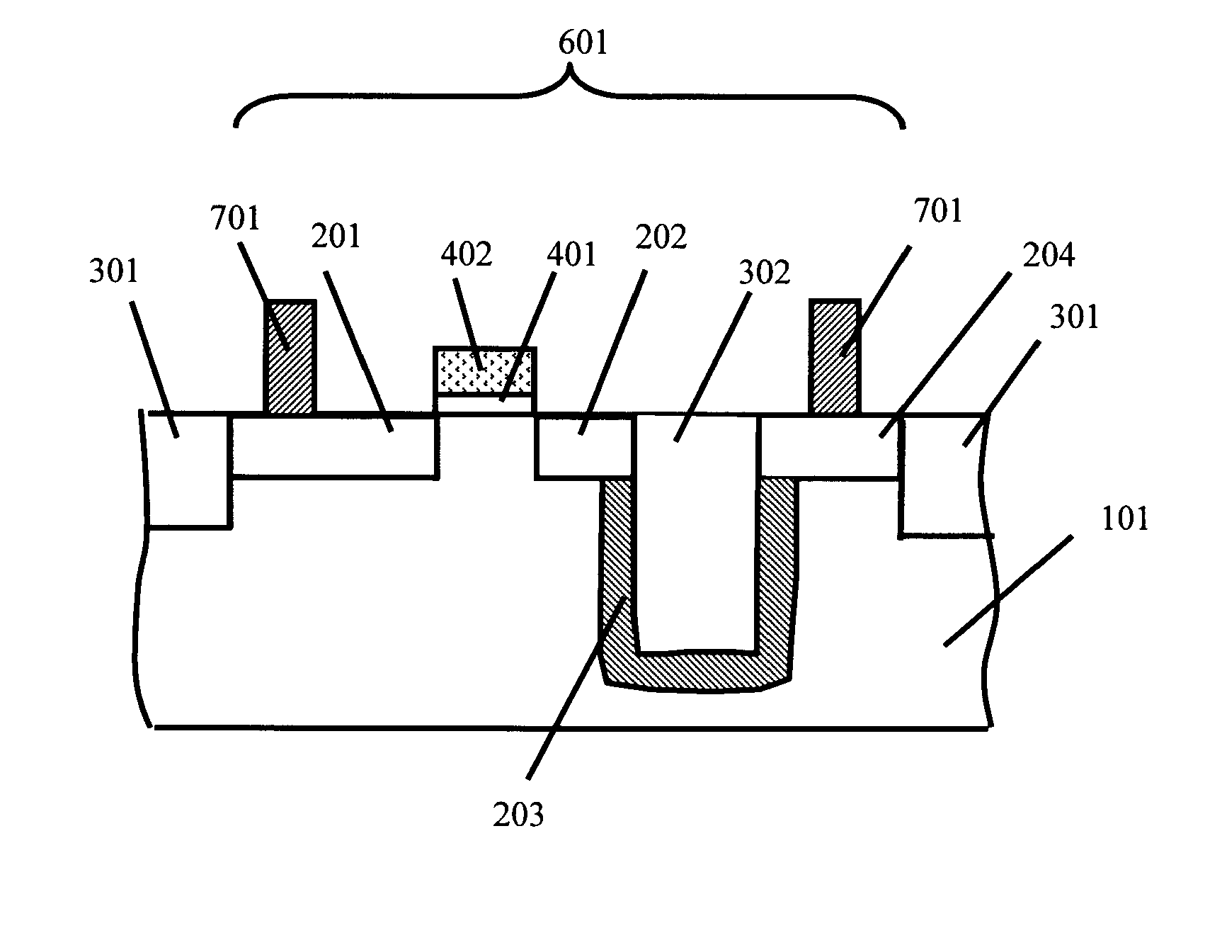
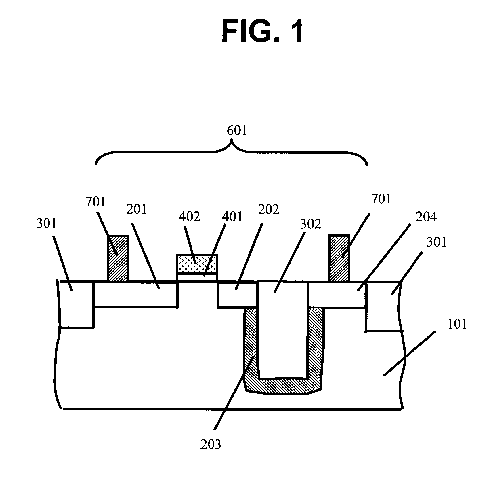
[0021]FIG. 1 is a schematic cross-sectional view illustrating an ESD protection N-type MOS transistor of a semiconductor device according to a first embodiment of the present invention.

[0022]On a P-type silicon substrate 101 as a semiconductor substrate of a first conductivity type, a source region 201 and a drain region 202 are formed of a pair of N-type heavily doped regions. Further, trench isolation regions 301 by shallow trench isolation are formed with respect to other elements, thereby achieving isolation.

[0023]Above a channel region of the P-type silicon substrate 101 between the source region 201 and the drain region 202, a gate electrode 402 made of a polysilicon film or the like is formed via a gate insulating film 401 made of a silicon oxide film or the like. In a region held in contact with the drain region 202, an ESD protection trench isolation region 302 is formed. The vertical depth of the ESD protection trench isolation region 302 is larger than the vertical depth ...

second embodiment

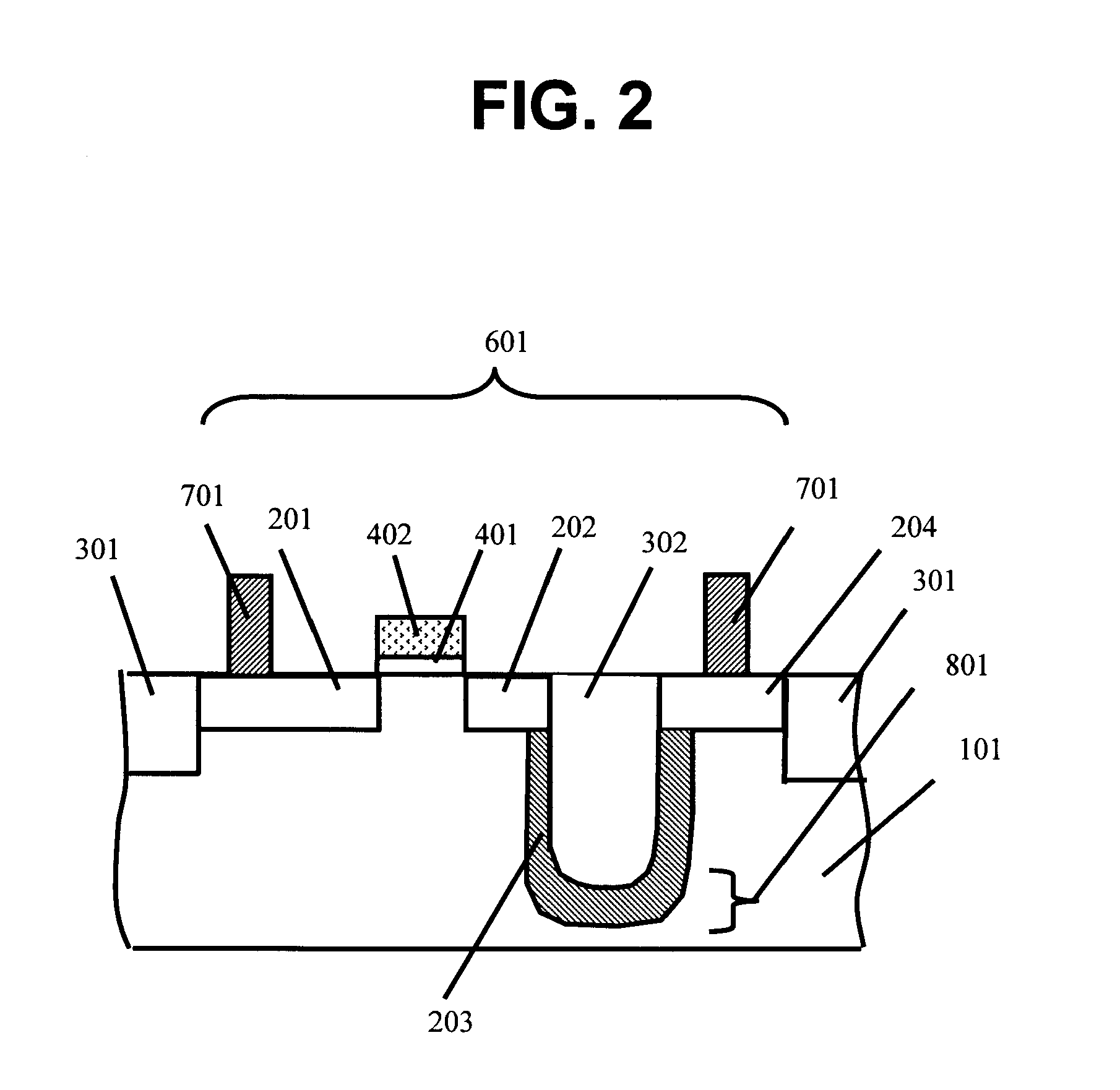
[0028]FIG. 2 is a schematic cross-sectional view illustrating an ESD protection N-type MOS transistor of a semiconductor device according to a second embodiment of the present invention.

[0029]The second embodiment is different from the first embodiment illustrated in FIG. 1 in that the bottom surface of the ESD protection trench isolation region 302 around which the drain extended region 203 is formed has rounded corners so that a rounded trench isolation region bottom surface 801 is formed.

[0030]In the case where a large forward current is applied from the outside, an effective drain region of an ESD protection N-type MOS transistor 601 for discharging the applied current as a forward current of a diode formed by junction of the N-type drain region and the P-type substrate of the ESD protection N-type MOS transistor 601 is a total region of the drain region 202, the drain extended region 203, and the drain contact region 204. As illustrated in FIG. 2, the bottom surface of the ESD ...


PUM


Abstract

In the semiconductor device including an ESD protection N-type MOS transistor having a sufficient ESD protective function, a drain region of the ESD protection N-type MOS transistor is electrically connected to a drain contact region via a drain extended region. The drain extended region is provided on a side surface and a lower surface of an ESD protection trench isolation region, and is formed of an impurity diffusion region of the same conductivity type as that of the drain region. The drain contact region is formed of an impurity diffusion region of the same conductivity type as that of the drain region.

Description

BACKGROUND OF THE INVENTION[0001]1. Field of the Invention[0002]The present invention relates to a semiconductor device including an electro-static discharge (ESD) protection element, which is formed between an external connection terminal and an internal circuit region in order to protect an internal element formed in the internal circuit region from being broken by ESD.[0003]2. Description of the Related Art[0004]In a semiconductor device including a MOS transistor, as an ESD protection element for preventing an internal circuit from being broken by static electricity from an external connection pad, an N-type MOS transistor which is provided so that a gate potential thereof is fixed to the ground (Vss) to be in an OFF state, that is, a so-called OFF transistor is known.[0005]In order to prevent ESD breakdown of an internal circuit element, it is important to draw as large a proportion as possible of an electrostatic pulse into the OFF transistor but not to propagate the electrost...

Claims


Application Information

Patent Timeline
Patent Type & Authority Applications(United States)
IPC IPC(8): H01L27/06
CPCH01L27/0617H01L29/0847H01L29/0653H01L29/7835H01L27/04
Inventor TAKASU, HIROAKI
Owner SEIKO INSTR INC
Why Eureka
Try Eureka