Method for manufacturing semiconductor device
a semiconductor film and manufacturing method technology, applied in the direction of semiconductor devices, basic electric elements, electrical appliances, etc., can solve the problems of reduced throughput, leakage current flow, and lengthening the formation time, so as to achieve efficient diffusion, reduce oxygen vacancies in the oxide semiconductor film, and efficiently diffuse
- Summary
- Abstract
- Description
- Claims
- Application Information
AI Technical Summary
Benefits of technology
Problems solved by technology
Method used
Image

Examples
embodiment 1
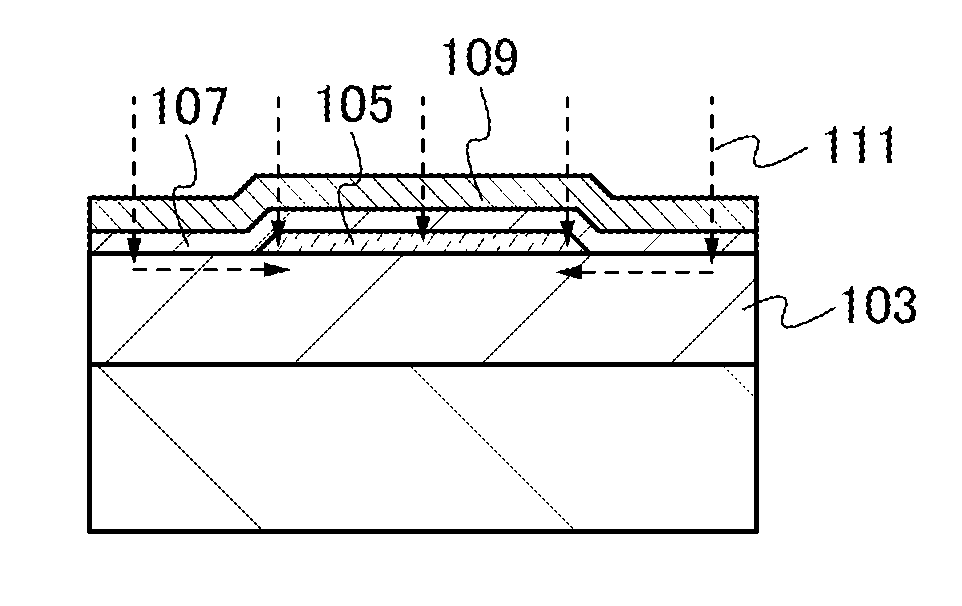
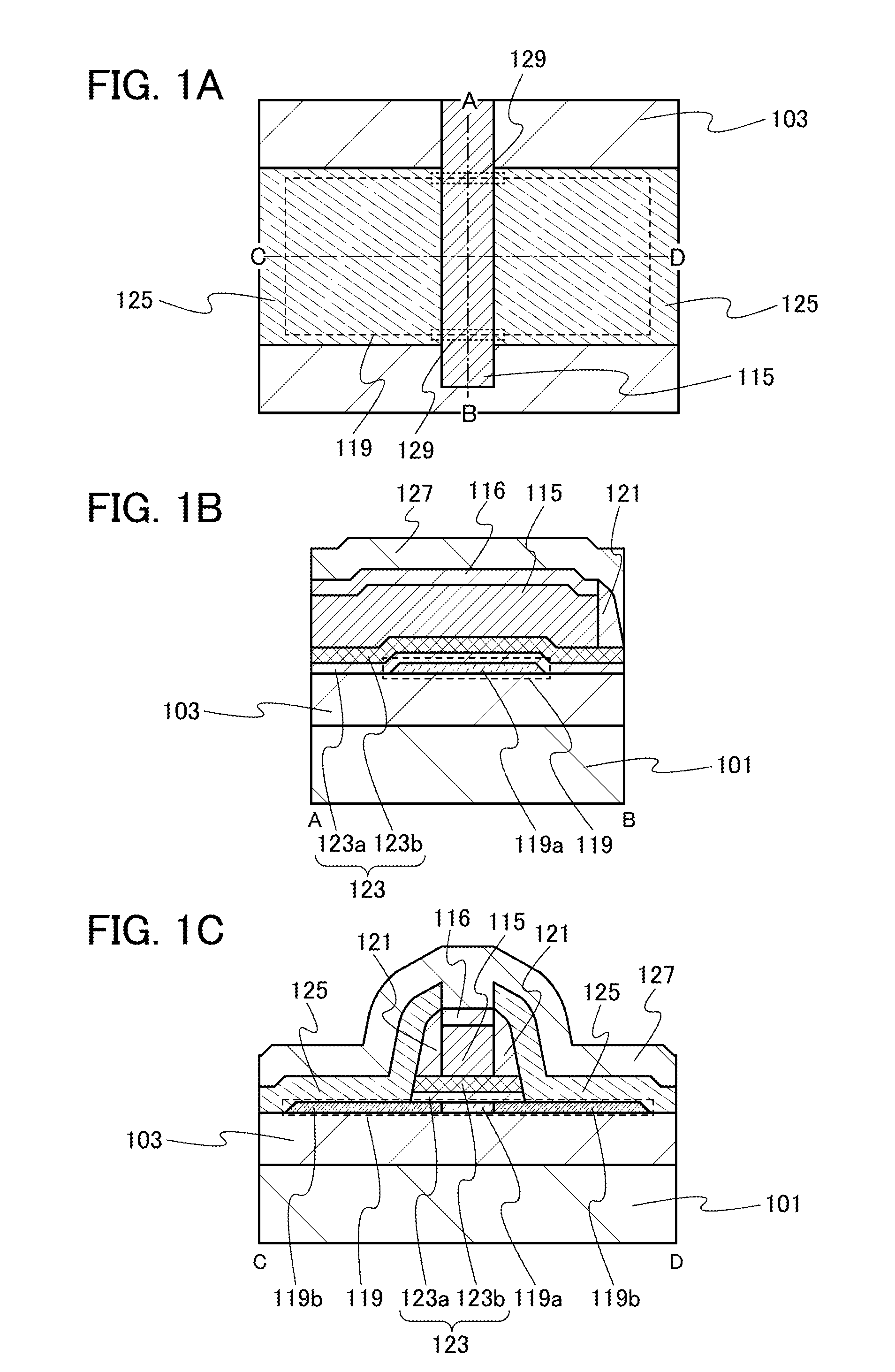
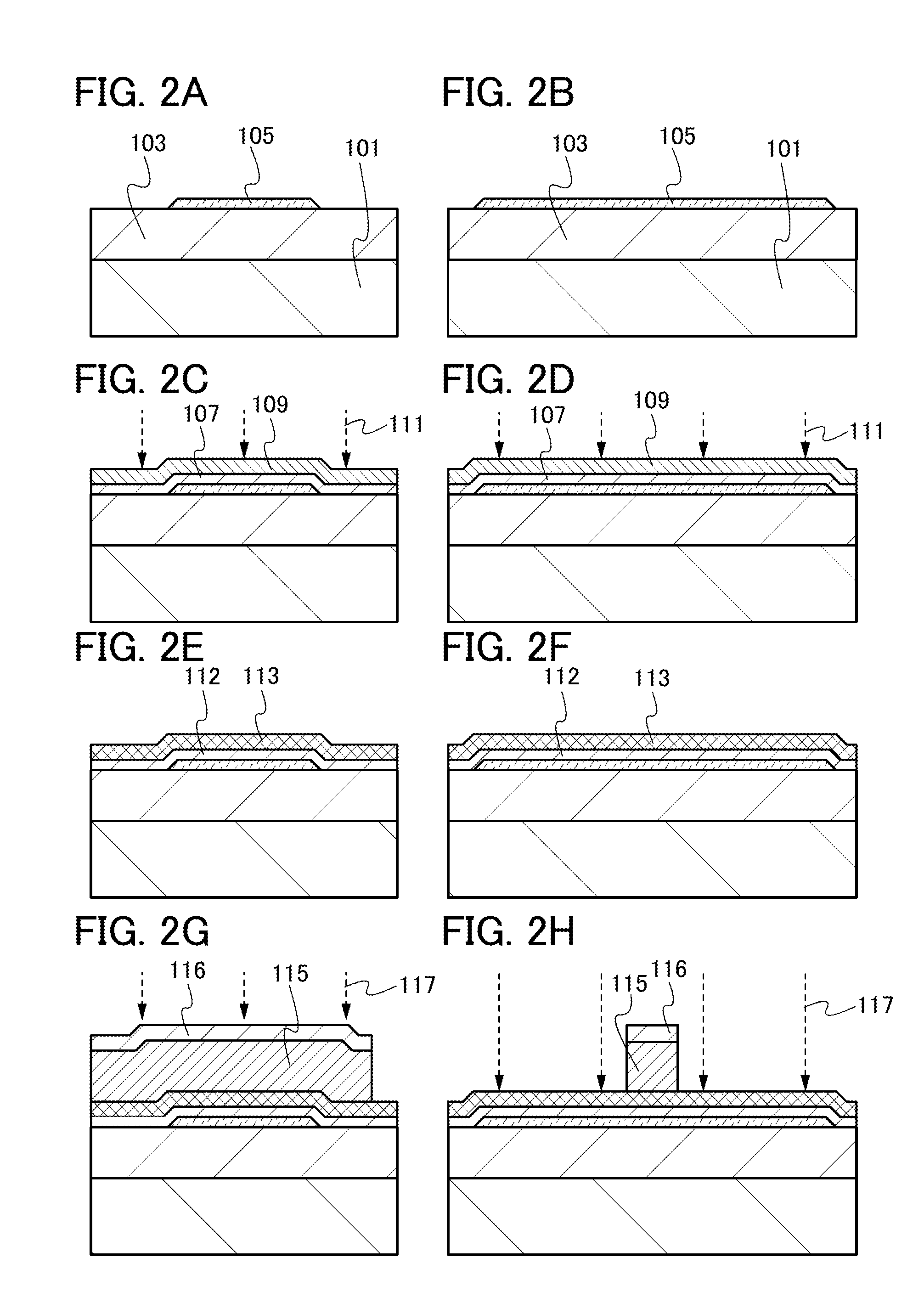
[0052]In this embodiment, a structure of a transistor having excellent electrical characteristics and a method for manufacturing the transistor with high productivity are described with reference to FIGS. 1A to 1C, FIGS. 2A to 2H, FIGS. 3A and 3B, FIGS. 4A to 4F, and FIGS. 5A and 5B.
[0053]FIGS. 1A to 1C are a top view and cross-sectional views of a transistor described in this embodiment. FIG. 1A is a top view of the transistor described in this embodiment. FIG. 1B is a cross-sectional view in the channel width direction of the transistor taken along dashed-dotted line A-B in FIG. 1A. FIG. 1C is a cross-sectional view in the channel length direction of the transistor taken along dashed-dotted line C-D in FIG. 1A. Note that in FIG. 1A, illustration of some components of the transistor (e.g., a gate insulating film 123, sidewall insulating films 121, an insulating film 116, and an insulating film 127) is omitted for clarity.
[0054]The transistor illustrated in FIGS. 1A to 1C includes a...
embodiment 2
[0221]In this embodiment, a transistor in which a metal oxide film formed by oxidizing a metal film is used as a gate insulating film and a method for manufacturing the transistor are described with reference to FIGS. 1A to 1C, FIGS. 2A to 2H, FIGS. 3A and 3B, FIGS. 4A to 4F, and FIGS. 5A and 5B. The transistor in this embodiment is different from that in Embodiment 1 in that only the metal oxide film formed by adding oxygen to a metal film is the gate insulating film.
[0222]FIGS. 5A and 5B are cross-sectional views of the transistor described in this embodiment. The top view of the transistor illustrated in FIGS. 5A and 5B is similar to that in FIG. 1A described in Embodiment 1, and thus is not illustrated here. FIG. 5A is a cross-sectional view in the channel width direction of the transistor, which corresponds to the dashed-dotted line A-B in FIG. 1A. FIG. 5B is a cross-sectional view in the channel length direction of the transistor, which corresponds to the dashed-dotted line C-...
embodiment 3
[0233]In this embodiment, a transistor in which a metal oxide film formed by oxidizing a metal film is used as a protective film for the transistor and a method for manufacturing the transistor are described with reference to FIGS. 1A to 1C, FIGS. 4A to 4F, and FIGS. 6A and 6B.
[0234]FIGS. 6A and 6B are cross-sectional views of the transistor described in this embodiment. The top view of the transistor illustrated in FIGS. 6A and 6B is similar to that in FIG. 1A described in Embodiment 1, and thus is not illustrated here. FIG. 6A is a cross-sectional view in the channel width direction of the transistor, which corresponds to the dashed-dotted line A-B in FIG. 1A. FIG. 6B is a cross-sectional view in the channel length direction of the transistor, which corresponds to the dashed-dotted line C-D in FIG. 1A.
[0235]The transistor illustrated in FIGS. 6A and 6B includes the oxide insulating film 103 over the substrate 101, the oxide semiconductor film 119 over the oxide insulating film 103...
PUM
 Abstract
Description
Claims
Application Information
 - R&D Engineer
- R&D Manager
- IP Professional
- Industry Leading Data Capabilities
- Powerful AI technology
- Patent DNA Extraction
Browse by: Latest US Patents, China's latest patents, Technical Efficacy Thesaurus, Application Domain, Technology Topic.
© 2024 PatSnap. All rights reserved.Legal|Privacy policy|Modern Slavery Act Transparency Statement|Sitemap