Electrostatic discharge protection structure for an active array substrate

Active Publication Date: 2013-08-15
E INK HLDG INC
View PDF4 Cites 6 Cited by
  • Summary
  • Abstract
  • Description
  • Claims
  • Application Information

AI Technical Summary

Benefits of technology

The present invention provides an electrostatic discharge protection structure that has stable electrical characteristics. The structure includes a signal line, a thin-film transistor, and a shunt wire. The thin-film transistor has a first thin-film transistor and a first drain electrode. The shunt wire is connected to the first drain electrode. The electrostatic discharge protection structure also includes a second thin-film transistor that connects the first drain electrode and the signal line. The second thin-film transistor has a second gate electrode, a second metal-oxide semiconductor layer, a second source electrode, and a second drain electrode. The electrostatic discharge protection structure may also include a third thin-film transistor that connects the third drain electrode and the signal line. The third thin-film transistor has a third gate electrode, a third metal-oxide semiconductor layer, a third source electrode, and a third drain electrode. The electrostatic discharge protection structure may also include a fourth thin-film transistor that connects the fifth drain electrode and the shunt wire. The electrostatic discharge protection structure helps to protect the signal line from electrostatic discharge and ensure stable operation of the signal line.

Problems solved by technology

However, the carrier mobility of the amorphous silicon semiconductor is unsatisfied, so that in many researches metal-oxide semiconductor material are promoted to replace the amorphous silicon semiconductor material.
Unfortunately, metal-oxide semiconductor material exhibits unstable characteristics.
Similar problems occur in the ESD protection structures that use metal-oxide semiconductor material, and cause the instabilities of ESD protection structures.

Method used


Image

  • Electrostatic discharge protection structure for an active array substrate
  • Electrostatic discharge protection structure for an active array substrate
  • Electrostatic discharge protection structure for an active array substrate

Examples


Embodiment Construction

[0022]Reference will now be made in detail to the present embodiments of the invention, examples of which are illustrated in the accompanying drawings. Wherever possible, the same reference numbers are used in the drawings and the description to refer to the same or like parts.

[0023]In the following detailed description, for purposes of explanation, numerous specific details are set forth in order to provide a thorough understanding of the disclosed embodiments. It will be apparent, however, that one or more embodiments may be practiced without these specific details. In other instances, well-known structures and devices are schematically shown in order to simplify the drawings.

[0024]The term “electrically connected to” in the present disclosure refers to an electrical connection that allows voltage and current to be transmitted through a physical and conductive path or circuit.

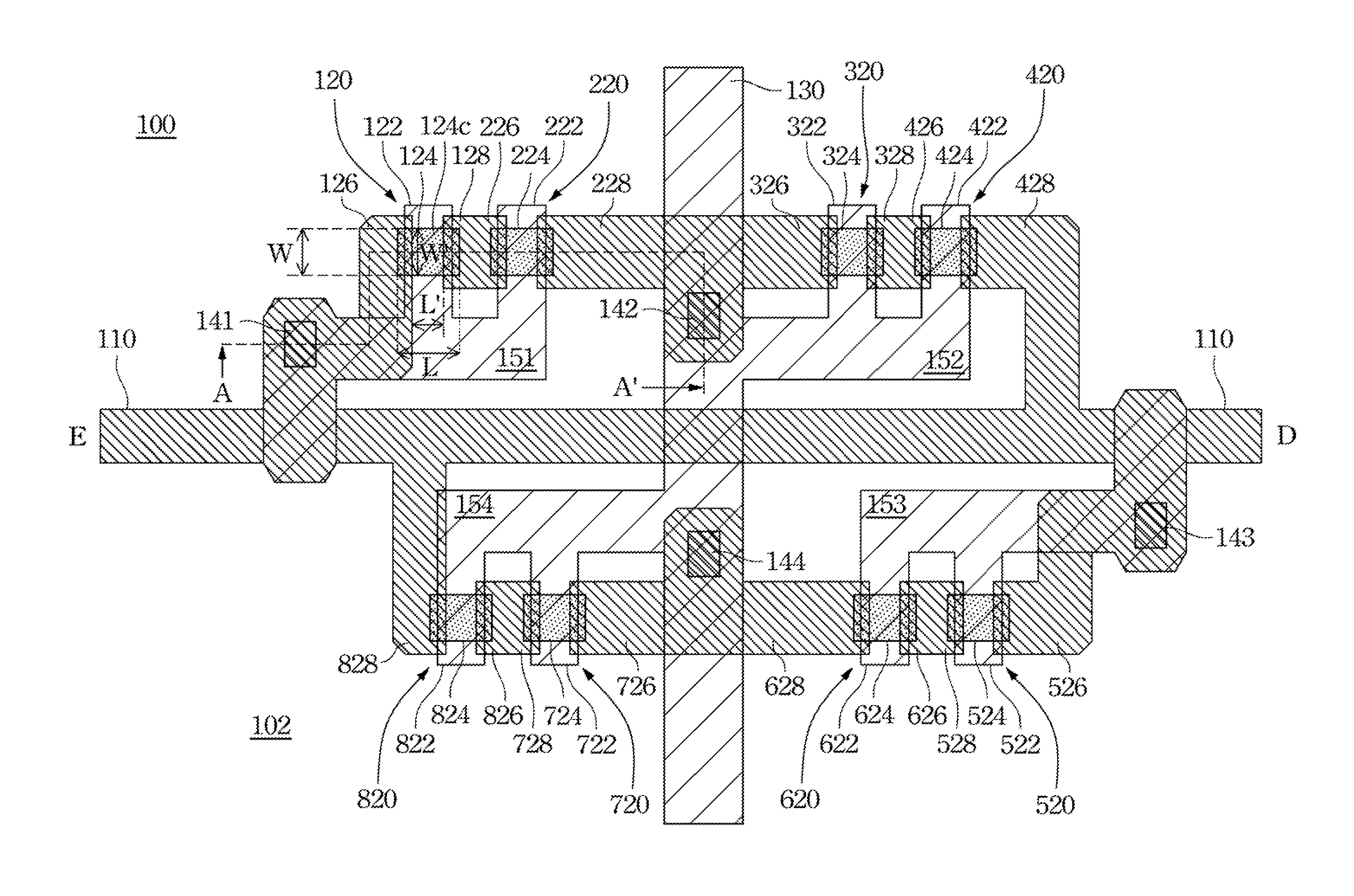
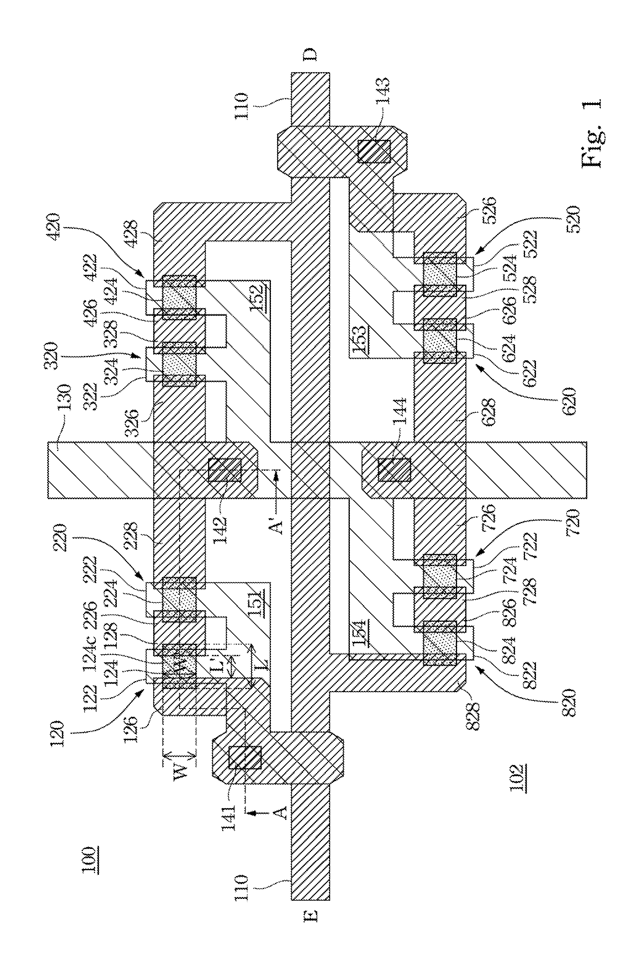
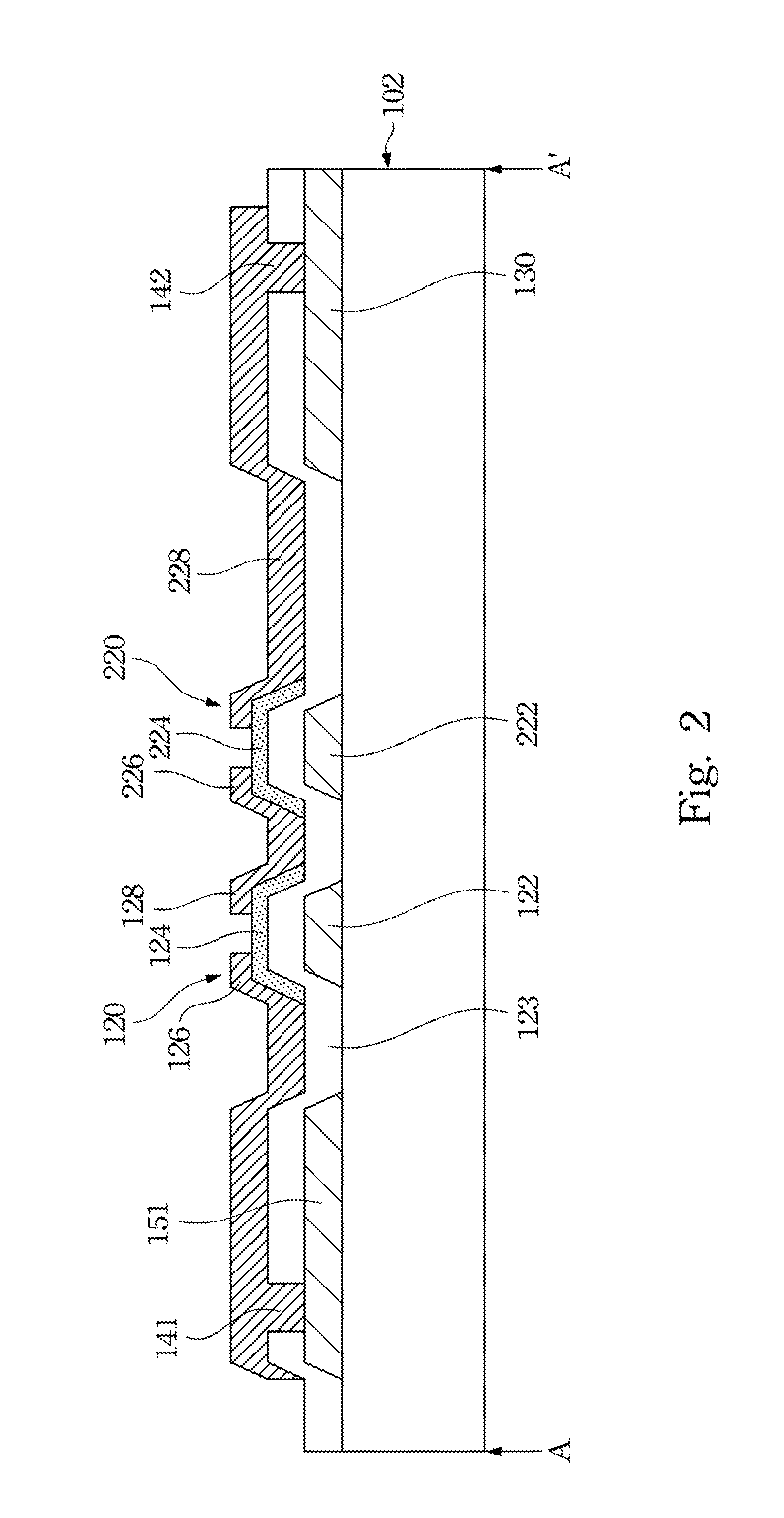
[0025]FIG. 1 is a top view schematically illustrating an electrostatic discharge (ESD) protection structur...


PUM


Abstract

Disclosed herein is an electrostatic discharge protection structure which includes a signal line, a thin-film transistor and a shunt wire. The thin-film transistor includes a gate electrode, a metal-oxide semiconductor layer, a source electrode and a drain electrode. The first metal-oxide semiconductor layer is disposed above the first gate electrode. The metal-oxide semiconductor layer has a channel region characterized in having a width / length ratio of less than 1. The source electrode is equipotentially connected to the gate electrode. The shunt wire is electrically connected to the drain electrode. When the signal line receives a voltage surge of greater than a predetermined magnitude, the voltage surge is shunted through the thin-film transistor to the shunt wire.

Description

CROSS REFERENCE TO RELATED APPLICATIONS[0001]This application claims priority to Taiwan Application Serial Number 101104429, filed Feb. 10, 2012, the disclosures of which are incorporated herein by reference in their entireties.BACKGROUND[0002]1. Technical Field[0003]The present invention relates to an electrostatic discharge (ESD) protection structure. More particularly, the present invention relates to an ESD protection structure formed on an active array substrate for a display device.[0004]2. Description of Related Art[0005]Liquid crystal display devices (LCDs) have been widely applied in various types of electronics. In the prior art, LCDs typically utilizes amorphous silicon thin-film transistors (TFTs) as active elements. In general, the active array substrates of LCDs include electrostatic discharge (ESD) protection structures to prevent the elements and circuits on the active array substrates from damage due to electrostatic voltage surges. Usually, the ESD protection struc...

Claims


Application Information

Patent Timeline
IPC IPC(8): H01L29/786
CPCH01L27/1225H01L29/786H01L27/0296
Inventor TSAI, XUE-HUNGYEH, CHIA-CHUNWANG, HENRYSHINN, TED-HONG
Owner E INK HLDG INC
Why Eureka
Try Eureka