Semiconductor device and manufacturing method thereof, module, and electronic device

Inactive Publication Date: 2016-04-21
SEMICON ENERGY LAB CO LTD
View PDF3 Cites 8 Cited by
  • Summary
  • Abstract
  • Description
  • Claims
  • Application Information

AI Technical Summary

Benefits of technology

[0013]An object is to provide a transistor with stable electrical characteristics. Another object is to provide a transistor with normally-off electrical characteristics. Another object is to provide a transistor with a small subthreshold swing value. Another object is to provide a transistor having a small short-chann

Problems solved by technology

For example, a display device in which a transistor including an ox

Method used


Image

  • Semiconductor device and manufacturing method thereof, module, and electronic device
  • Semiconductor device and manufacturing method thereof, module, and electronic device
  • Semiconductor device and manufacturing method thereof, module, and electronic device

Examples


example 1

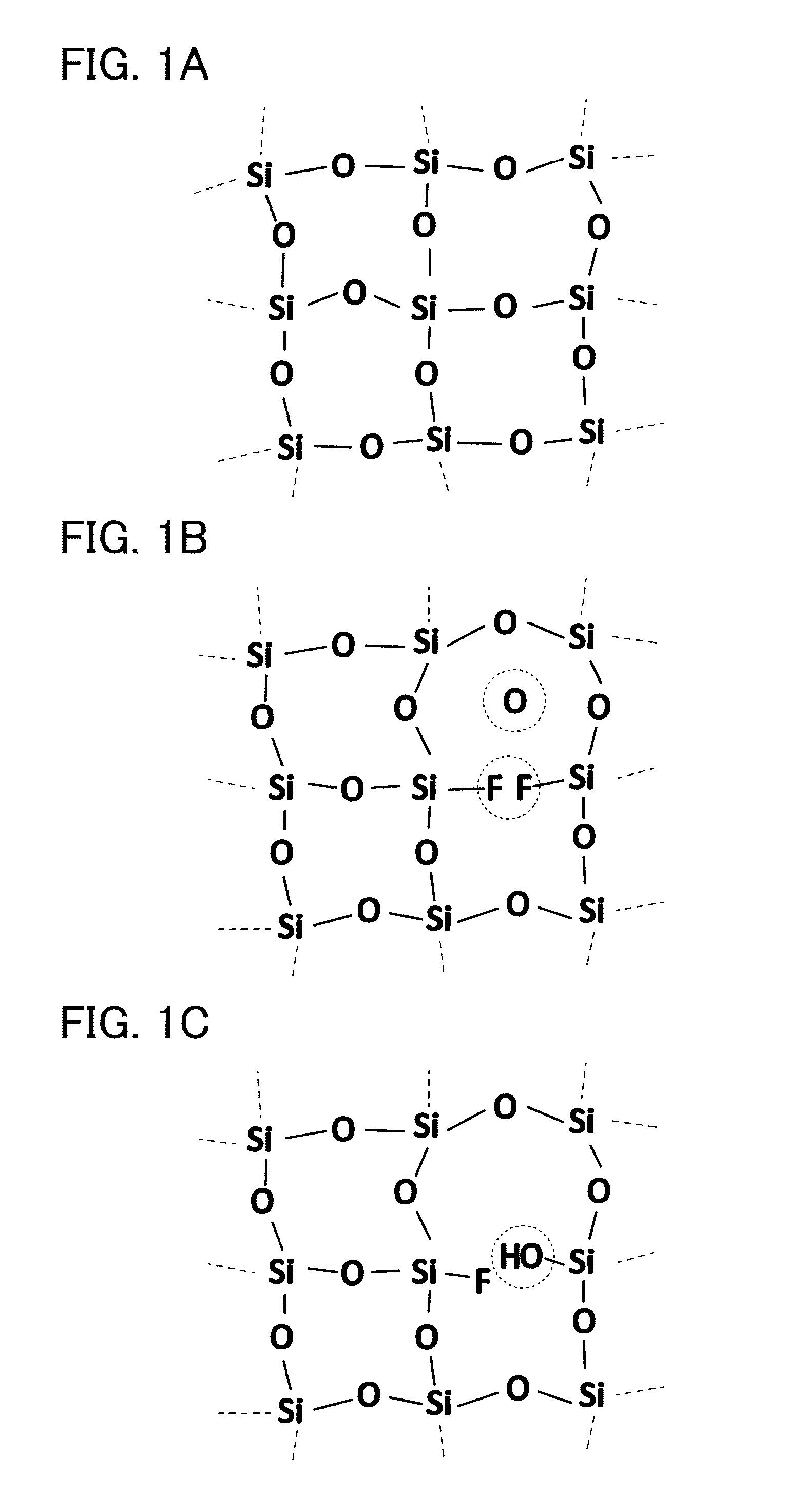
[0566]In this example, it was verified whether excess oxygen is formed by adding fluorine to a silicon oxide.

[0567]A sample was fabricated in such a manner that a 100-nm-thick silicon oxide film was formed over a silicon substrate by a thermal oxidation method.

[0568]By an ion implantation method, 19F+ ions with a dose of 1.0×10¹⁶ ions / cm2 was added to the sample. Note that the accelerating voltage was 10 kV. FIG. 69 shows the calculation value of the amount of added fluorine in the depth direction. FIG. 69 also shows the amounts of added fluorine in the depth direction with accelerating voltages of 15 kV and 20 kV as reference values. For the calculation, SRIM, the Stopping and Range of Ions in Matter, was used. The silicon oxide here had two oxygen atoms with respect to one silicon atom. The density of the silicon oxide was 2.2 g / cm3.

[0569]FIG. 70 shows changes in fluorine concentration in the depth direction of a sample to which fluorine was added (referred to as Example Sample) a...


PUM


Abstract

A transistor with stable electrical characteristics or a transistor with normally-off electrical characteristics. The transistor is a semiconductor device including a conductor, a semiconductor, a first insulator, and a second insulator. The semiconductor is over the first insulator. The conductor is over the semiconductor. The second insulator is between the conductor and the semiconductor. The first insulator includes fluorine and hydrogen. The fluorine concentration of the first insulator is higher than the hydrogen concentration of the first insulator.

Description

TECHNICAL FIELD[0001]The present invention relates to, for example, a transistor or a semiconductor device. The present invention relates to, for example, a method for manufacturing a transistor or a semiconductor device. The present invention relates to, for example, a display device, a light-emitting device, a lighting device, a power storage device, a memory device, a processor, or an electronic device. The present invention relates to a method for manufacturing a display device, a liquid crystal display device, a light-emitting device, a memory device, or an electronic device. The present invention relates to a driving method of a display device, a liquid crystal display device, a light-emitting device, a memory device, or an electronic device.[0002]Note that one embodiment of the present invention is not limited to the above technical field. The technical field of one embodiment of the invention disclosed in this specification and the like relates to an object, a method, or a m...

Claims


Application Information

Patent Timeline
IPC IPC(8): H01L29/786H01L29/66
CPCH01L29/66969H01L29/7869H01L27/1225H01L29/41733H01L29/45H01L29/4908H01L29/78606H01L29/78618H01L29/78648H01L29/78696
Inventor YAMAZAKI, SHUNPEISHIMOMURA, AKIHISAYAMANE, YASUMASAYAMADE, NAOTOTANAKA, TETSUHIRO
Owner SEMICON ENERGY LAB CO LTD
Why Eureka
Try Eureka