Process for fabricating a silicon-on-insulator structure

a technology of silicon-on-insulator and fabrication process, which is applied in the direction of semiconductor devices, semiconductor/solid-state device details, electrical apparatus, etc., can solve the problems of risk of further amplification, and achieve the effect of increasing the amount of water present and increasing the bond strength

Active Publication Date: 2013-08-15
SOITEC SA
View PDF5 Cites 13 Cited by
  • Summary
  • Abstract
  • Description
  • Claims
  • Application Information

AI Technical Summary

Benefits of technology

[0050]To produce such a bond, and with a view to closing the bonding interface, it is known to plasma activate the surface of the oxide. The plasma activation is intended to increase the bond strength.
[0051]However, such an activation increases the amount of water present at the interface and therefore risks further amplifying the bubbling effect that it is desired to prevent.

Problems solved by technology

However, such an activation increases the amount of water present at the interface and therefore risks further amplifying the bubbling effect that it is desired to prevent.

Method used


Image

  • Process for fabricating a silicon-on-insulator structure
  • Process for fabricating a silicon-on-insulator structure
  • Process for fabricating a silicon-on-insulator structure

Examples


Embodiment Construction

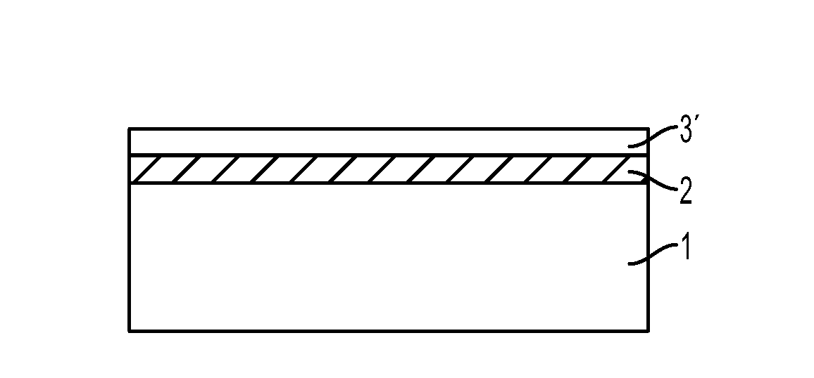
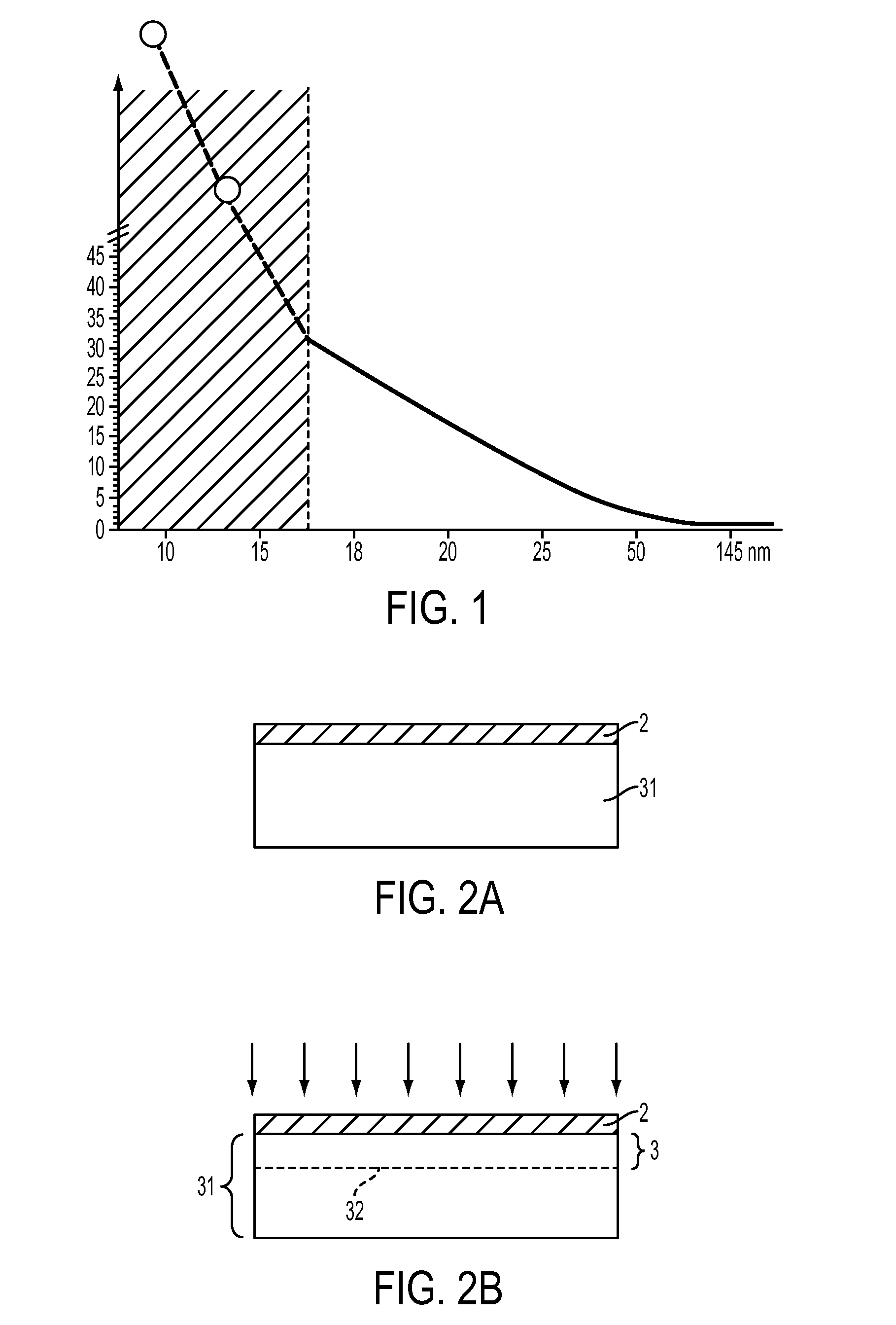
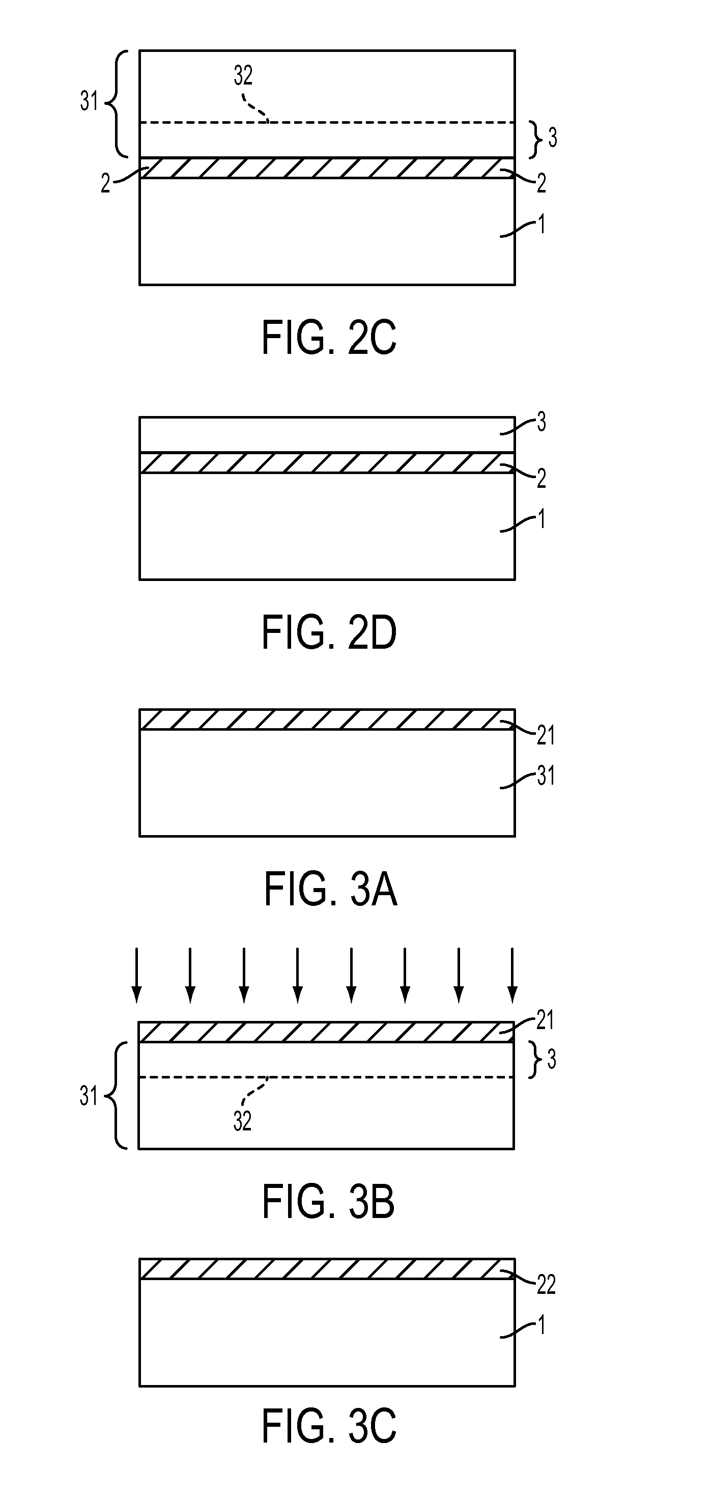
[0083]The fabrication of a silicon-on-insulator structure having a buried oxide layer that is 25 nm or less in thickness will now be described.

[0084]To form such a structure, a donor substrate is provided from which a silicon layer, intended to form the ultrathin layer of the SOI wafer, may be transferred.

[0085]In so far as the final ultrathin layer results from thinning the transferred layer after the cleaving process, the thickness of the silicon layer transferred from the donor substrate is substantially larger than the thickness of the final silicon layer of the SOI substrate.

[0086]Thus, to form the ultrathin layer of silicon of an SOI substrate (i.e., having a thickness of 50 nm or less), a silicon layer having a thickness of 600 nm or less may be transferred from the donor substrate.

[0087]The donor substrate may be a single-crystal bulk silicon substrate.

[0088]Alternatively, the donor substrate may be a composite substrate. In other words, the donor substrate may comprise a mu...


PUM


Abstract

Embodiments of to invention relate to a process for fabricating a silicon-on-insulator structure comprising the following steps: providing a donor substrate and a support substrate, only one of the substrates being covered with an oxide layer; forming, in the donor substrate, a weak zone; plasma activating the oxide layer; bonding the donor substrate to the support substrate in a partial vacuum; implementing a bond-strengthening anneal at a temperature of 350° C. or less causing the donor substrate to cleave along the weak zone; and carrying out a heat treatment at a temperature above 900° C. A transition from the temperature of the bond-strengthening anneal to the temperature of the heat treatment may be achieved at a ramp rate above 10° C. / s.

Description

CROSS-REFERENCE TO RELATED APPLICATION[0001]This application claims the benefit under 35 U.S.C. §119(a) of French Patent Application FR1158898, filed Oct. 3, 2011, and entitled “Process for Fabricating a Silicon-On-Insulator Structure,” the disclosure of which is hereby incorporated herein by this reference in its entirety.TECHNICAL FIELD[0002]The present invention relates to a silicon-on-insulator structure comprising a silicon layer, a buried oxide layer the thickness of which is 25 nm or less, and a support substrate, and to a process for fabricating such a structure.BACKGROUND[0003]Silicon-on-Insulator (SOI) structures are frequently used in Complementary Metal-Oxide-Semiconductor (CMOS) applications.[0004]Such structures comprise, from their useful surface to their bottom side: a thin silicon layer; a buried layer made of a dielectric material that is typically an oxide, such as SiO2; and a support substrate. The buried layer made of a dielectric material is often denoted by th...

Claims


Application Information

Patent Timeline
Patent Type & Authority Applications(United States)
IPC IPC(8): H01L21/762H01L29/06
CPCH01L21/76254H01L29/06H01L21/3105H01L21/20H01L27/12H01L21/7624H01L21/76251
Inventor DAVID, CAROLEKERDILES, SEBASTIEN
Owner SOITEC SA
Why Eureka
Try Eureka