Method for achieving sustained anisotropic crystal growth on the surface of a silicon melt

a silicon melt and anisotropic crystal technology, applied in the direction of crystal growth process, polycrystalline material growth, under a protective fluid, etc., can solve the problems of large temperature gradient along the ribbon, poor quality multi-grain silicon, and the wafer or sheet used in the manufacture of solar cells

Inactive Publication Date: 2013-08-22
LEADING EDGE CRYSTAL TECH INC
View PDF5 Cites 12 Cited by
  • Summary
  • Abstract
  • Description
  • Claims
  • Application Information

AI Technical Summary

Problems solved by technology

One major cost in the solar cell industry is the wafer or sheet used to make these solar cells.
This results in a large temperature gradient along the ribbon.
This temperature gradient stresses the crystalline silicon ribbon and may result in poor quality multi-grain silicon.
The width and thickness of the ribbon also may be limited due to this temperature gradient.
These early attempts have not met the goal of producing a reliable and rapidly drawn wide ribbon with uniform thickness that is “production worthy.”
Although radiative cooling of a silicon melt has been proposed as an alternative method of forming crystalline silicon, a problem arises because the large difference in emissivityεs−εl between solid and liquid silicon makes it difficult to obtain rapid solidification of the melt surface using radiative cooling.

Method used


Image

  • Method for achieving sustained anisotropic crystal growth on the surface of a silicon melt
  • Method for achieving sustained anisotropic crystal growth on the surface of a silicon melt
  • Method for achieving sustained anisotropic crystal growth on the surface of a silicon melt

Examples


Embodiment Construction

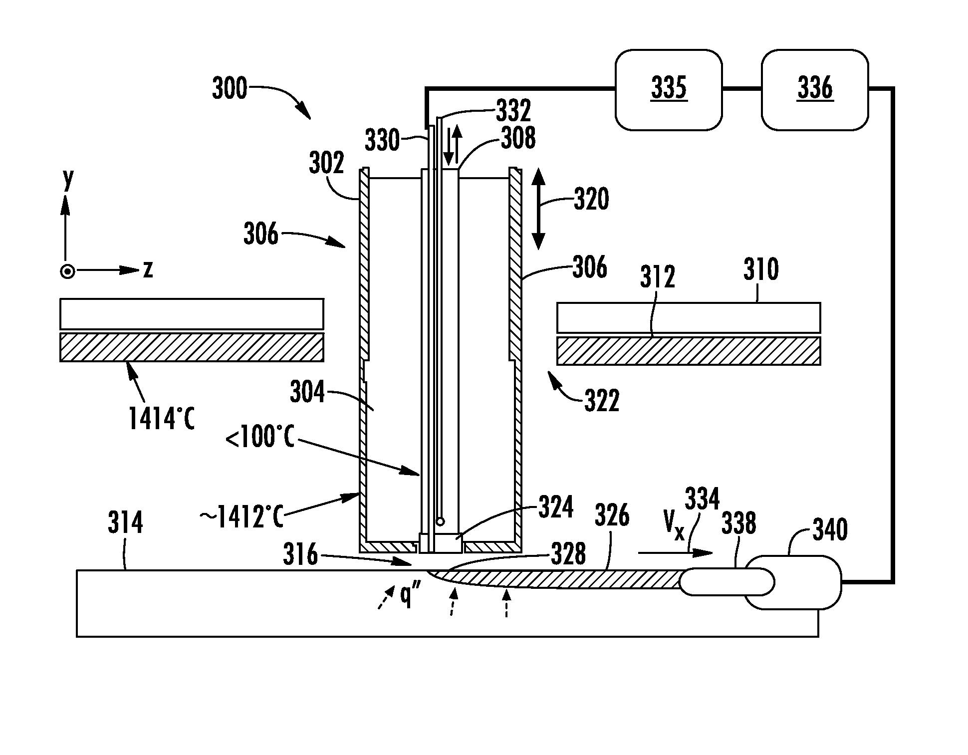
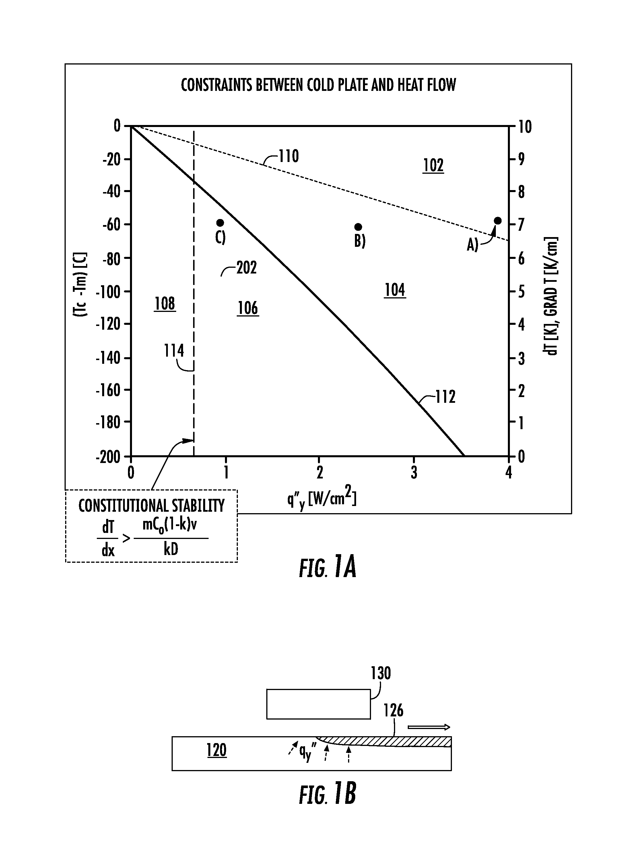
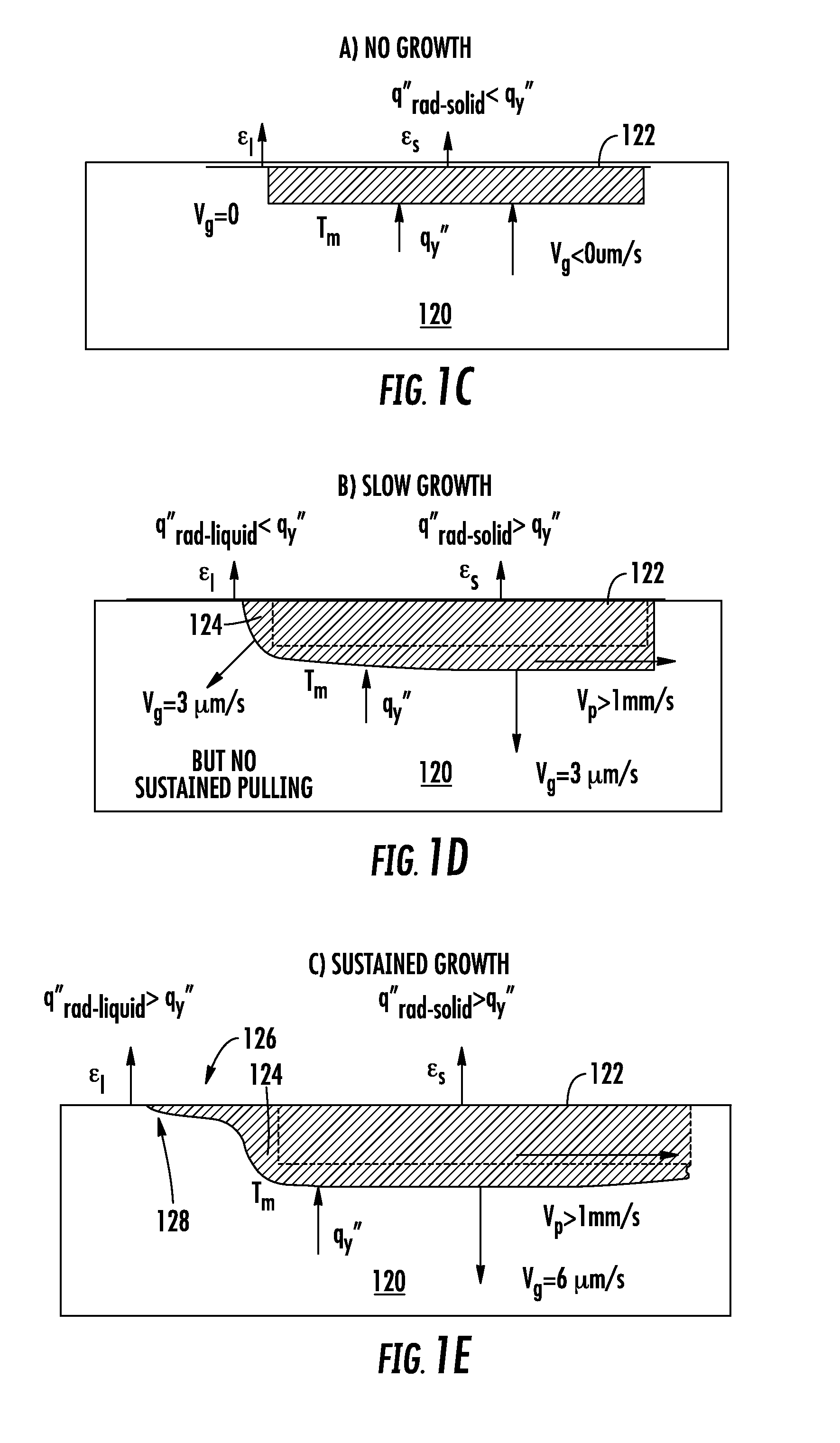
[0027]The present invention will now be described more fully hereinafter with reference to the accompanying drawings, in which preferred embodiments of the invention are shown. This invention, however, may be embodied in many different forms and should not be construed as limited to the embodiments set forth herein. Rather, these embodiments are provided so that this disclosure will be thorough and complete, and will fully convey the scope of the invention to those skilled in the art. In the drawings, like numbers refer to like elements throughout.

[0028]To solve the deficiencies associated with the methods noted above, the present embodiments provide novel and inventive apparatus and techniques for horizontal melt growth of a crystalline material, in particular, a monocrystalline material. In various embodiments apparatus for forming a sheet of monocrystalline silicon by horizontal melt growth are disclosed, though other materials, compounds, or alloys may be used. The apparatus dis...


PUM

PropertyMeasurementUnit
temperatureaaaaaaaaaa
surface temperatureaaaaaaaaaa
melting temperatureaaaaaaaaaa

Abstract

An apparatus for growing a crystalline sheet from a melt includes a cold block assembly. The cold block assembly may include a cold block and a shield surrounding the cold block and being at an elevated temperature with respect to that of the cold block, the shield defining an opening disposed along a surface of the cold block proximate a melt surface that defines a cold area comprising a width along a first direction of the cold block, the cold area operable to provide localized cooling of a region of the melt surface proximate the cold block. The apparatus may further include a crystal puller arranged to draw a crystalline seed in a direction perpendicular to the first direction when the cold block assembly is disposed proximate the melt surface.

Description

STATEMENT AS TO FEDERALLY SPONSORED RESEARCH OR DEVELOPMENT[0001]The U.S. Government has a paid-up license in this invention and the right in limited circumstances to require the patent owner to license others on reasonable terms as provided for by the terms of contract number DE-EE0000595 awarded by the U.S. Department of Energy.BACKGROUND OF THE INVENTION[0002]1. Field of the Invention[0003]Embodiments of the invention relate to the field of substrate manufacturing. More particularly, the present invention relates to a method, system and structure for growing a crystal sheet from a melt.[0004]2. Discussion of Related Art[0005]Silicon wafers or sheets may be used in, for example, the integrated circuit or solar cell industry. Demand for solar cells continues to increase as the demand for renewable energy sources increases. One major cost in the solar cell industry is the wafer or sheet used to make these solar cells. Reductions in cost to the wafers or sheets will, consequently, re...

Claims


Application Information

Patent Timeline
Patent Type & Authority Applications(United States)
IPC IPC(8): C30B15/20C30B15/00
CPCC30B15/06C30B15/14Y10T117/1008Y10T117/1068C30B29/06Y10T117/1044Y10T117/1048
Inventor MACKINTOSH, BRIAN H.KELLERMAN, PETER L.SUN, DAWEI
Owner LEADING EDGE CRYSTAL TECH INC
Why Eureka
Try Eureka