Semiconductor packages

a technology of semiconductors and packages, applied in the field of semiconductor packages, can solve problems such as electromagnetic interference in electronic devices or systems, deterioration of the overall performance of the device, and malfunction of the device, and achieve the effect of increasing the reliability of operation

Active Publication Date: 2013-08-22
SAMSUNG ELECTRONICS CO LTD
View PDF7 Cites 63 Cited by
  • Summary
  • Abstract
  • Description
  • Claims
  • Application Information

AI Technical Summary

Benefits of technology

[0006]Example embodiments of the inventive concept may provide a semiconductor package with increased operational reliability.

Problems solved by technology

Electronic devices or systems may be suffer from electromagnetic interference (EMI), which may result from a radiated emission (RE) or a conducted emission (CE) unnecessarily occurring in the electronic devices.
For example, the electromagnetic interference may disturb the operation of other electronic devices adjacent thereto, thereby deteriorating overall performance of the device or causing the malfunctioning of the device.

Method used


Image

  • Semiconductor packages
  • Semiconductor packages
  • Semiconductor packages

Examples


Embodiment Construction

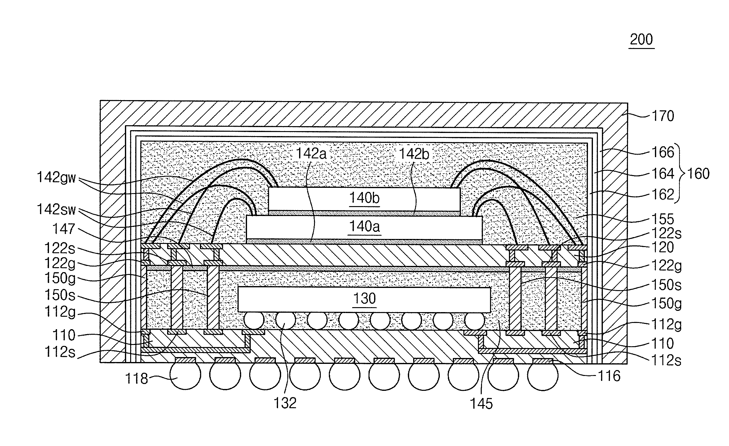
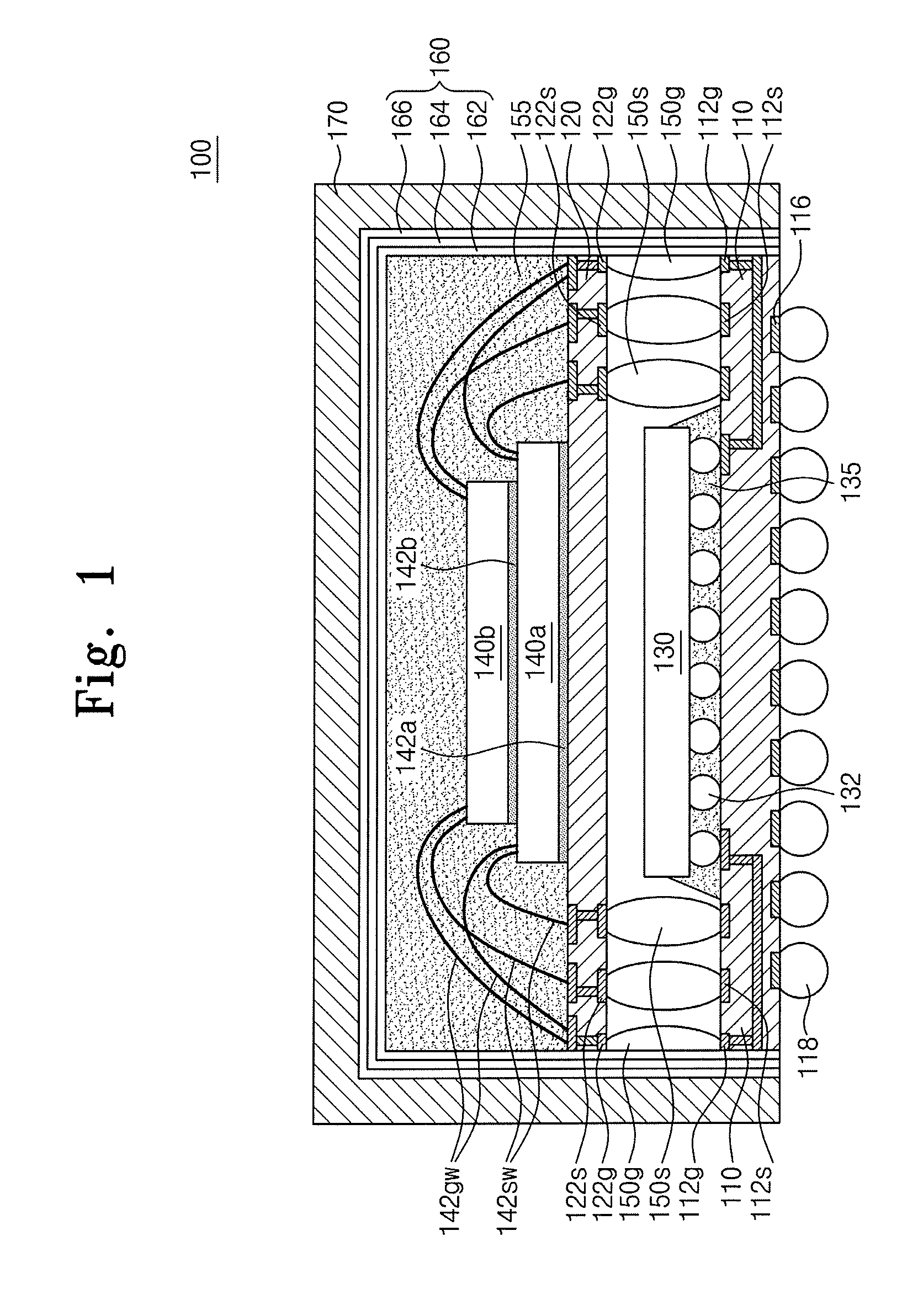
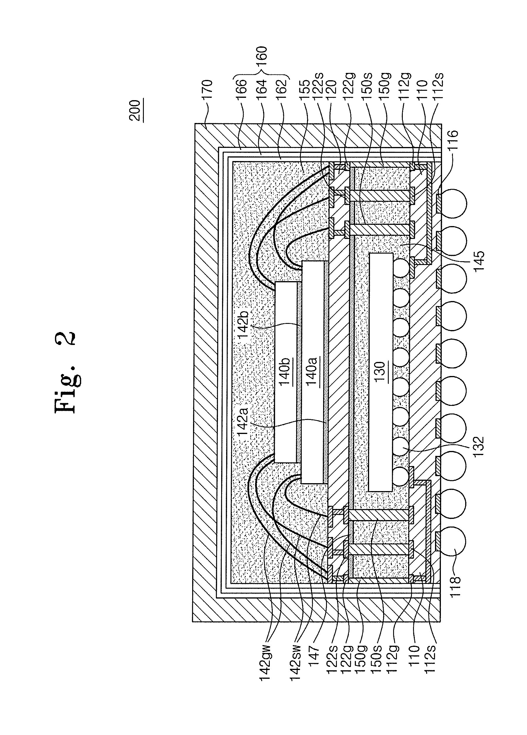
[0029]Example embodiments of the inventive concept will now be described more fully with reference to the accompanying drawings, in which example embodiments are shown. Example embodiments of the inventive concepts may, however, be embodied in many different forms and should not be construed as being limited to embodiments set forth herein. In the drawings, the thicknesses of layers and regions may be exaggerated for clarity. Like reference numerals in the drawings denote like elements, and thus their description will be omitted.

[0030]It will be understood that when an element is referred to as being “connected” or “coupled” to another element, it can be directly connected or coupled to the other element or intervening elements may be present. As used herein the term “and / or” includes any and all combinations of one or more of the associated listed items.

[0031]The terminology used herein is for the purpose of describing particular embodiments only and is not intended to be limiting ...


PUM


Abstract

A semiconductor package includes a first package including a first wiring board and at least one first semiconductor chip mounted on the first wiring board, a second package stacked on the first package. The second package includes a second wiring board and at least one second semiconductor chip mounted on the second wiring board. The semiconductor package further includes at least one connection terminal connecting a plurality of signal lines of the first and second wiring boards, respectively, with each other. The semiconductor package further includes at least one ground terminal connecting a plurality of ground lines of the first and second wiring boards, respectively, with each other, and includes a side surface, and a shielding member covering a top surface and a side surface of a structure including the first and second packages and the shielding member is disposed on the at least one ground terminal.

Description

CROSS-REFERENCE TO RELATED APPLICATIONS[0001]This application claims priority to Korean Patent Application No. 10-2012-0015847, filed on Feb. 16, 2012, the disclosure of which is hereby incorporated by reference herein in its entirety.(i) TECHNICAL FIELD[0002]Example embodiments of the inventive concept relate to a semiconductor package, and more particularly, to a semiconductor package with package-on-package structure.(ii) DISCUSSION OF THE RELATED ART[0003]There is a growing trend to fabricate lightweight, small-sized, high speed, multifunctional, high performance, and low-cost electronic systems. In response to such a trend, multi-chip stacked package techniques and / or system in package techniques have been proposed.[0004]In a multi-chip stacked package or a system in package, one or more functions of a plurality of semiconductor devices may be performed in a single semiconductor package. A multi-chip stacked package or a system in package may have a thicker thickness compared t...

Claims


Application Information

Patent Timeline
Patent Type & Authority Applications(United States)
IPC IPC(8): H01L23/552
CPCH01L2225/06537H01L2224/48091H01L24/16H01L24/32H01L24/48H01L24/73H01L25/105H01L2224/16225H01L2224/32145H01L2224/32225H01L2224/48227H01L2224/73204H01L2224/73265H01L2225/0651H01L2225/1023H01L2225/1058H01L2225/1094H01L2924/14335H01L2924/1436H01L2924/1437H01L2924/1438H01L2924/15192H01L2924/15311H01L2924/15331H01L2225/06568H01L23/552H01L2924/3025H01L2924/07802H01L2924/00012H01L2924/00014H01L2924/00H01L2924/12042H01L2924/181H01L2224/45099H01L2224/45015H01L2924/207H01L23/12H01L23/60
Inventor KIM, YONGHOON
Owner SAMSUNG ELECTRONICS CO LTD
Why Eureka
Try Eureka