Fabrication method for improving surface planarity after tungsten chemical mechanical polishing

Active Publication Date: 2013-08-29
SHANGHAI HUALI MICROELECTRONICS CORP
View PDF2 Cites 2 Cited by
  • Summary
  • Abstract
  • Description
  • Claims
  • Application Information

AI Technical Summary

Benefits of technology

The present invention provides a method of fabricating semiconductor devices by forming contact holes and dummy patterns with two photolithography-and-etching processes, and then filling them with tungsten and removing the redundant tungsten. This method reduces wiring density differences between different areas and improves surface planarity, preventing metal residue formation and improving device performance. Additionally, a reduction in metal filled in dummy patterns close to gate electrodes or active-area silicides prevents any impact on device performance.

Problems solved by technology

However, in a Cu-CMP process, non-uniformity of copper wiring density will lead to defects, such as dishing 2 and erosion 1 shown in FIG. 1, in certain areas, for example, where wires are relatively wide, or where wiring densities are relatively high.
These defects will affect post-CMP surface planarity and hence lower the production yield and reliability.
On the other hand, in the case of multilayer wiring, CMP process itself also requires a good surface planarity, because surface non-planarity will accumulate with the increase of layers and may finally lead to the metal residue or defects, such as pooling and bridging, in certain areas during subsequent processes of forming copper interconnections.

Method used


Image

  • Fabrication method for improving surface planarity after tungsten chemical mechanical polishing
  • Fabrication method for improving surface planarity after tungsten chemical mechanical polishing
  • Fabrication method for improving surface planarity after tungsten chemical mechanical polishing

Examples


Embodiment Construction

[0025]Foregoing objectives, characteristics and advantages of the present invention will be clearer and easier to be understood upon reading the following description of specific embodiments with reference to the accompanying drawings.

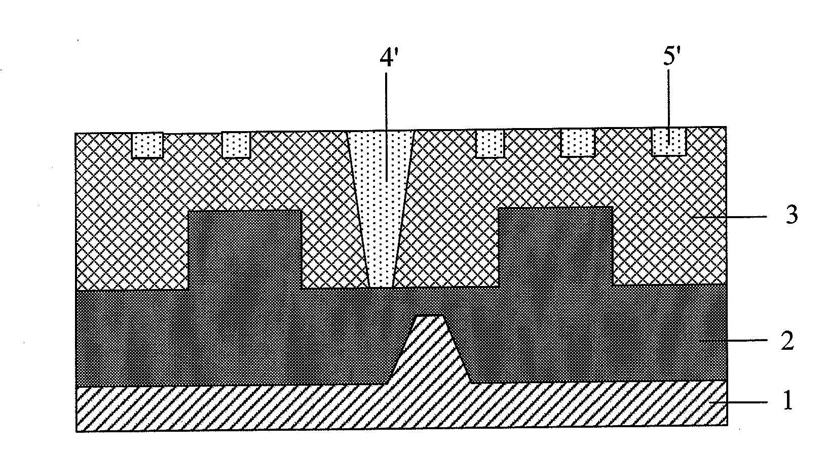
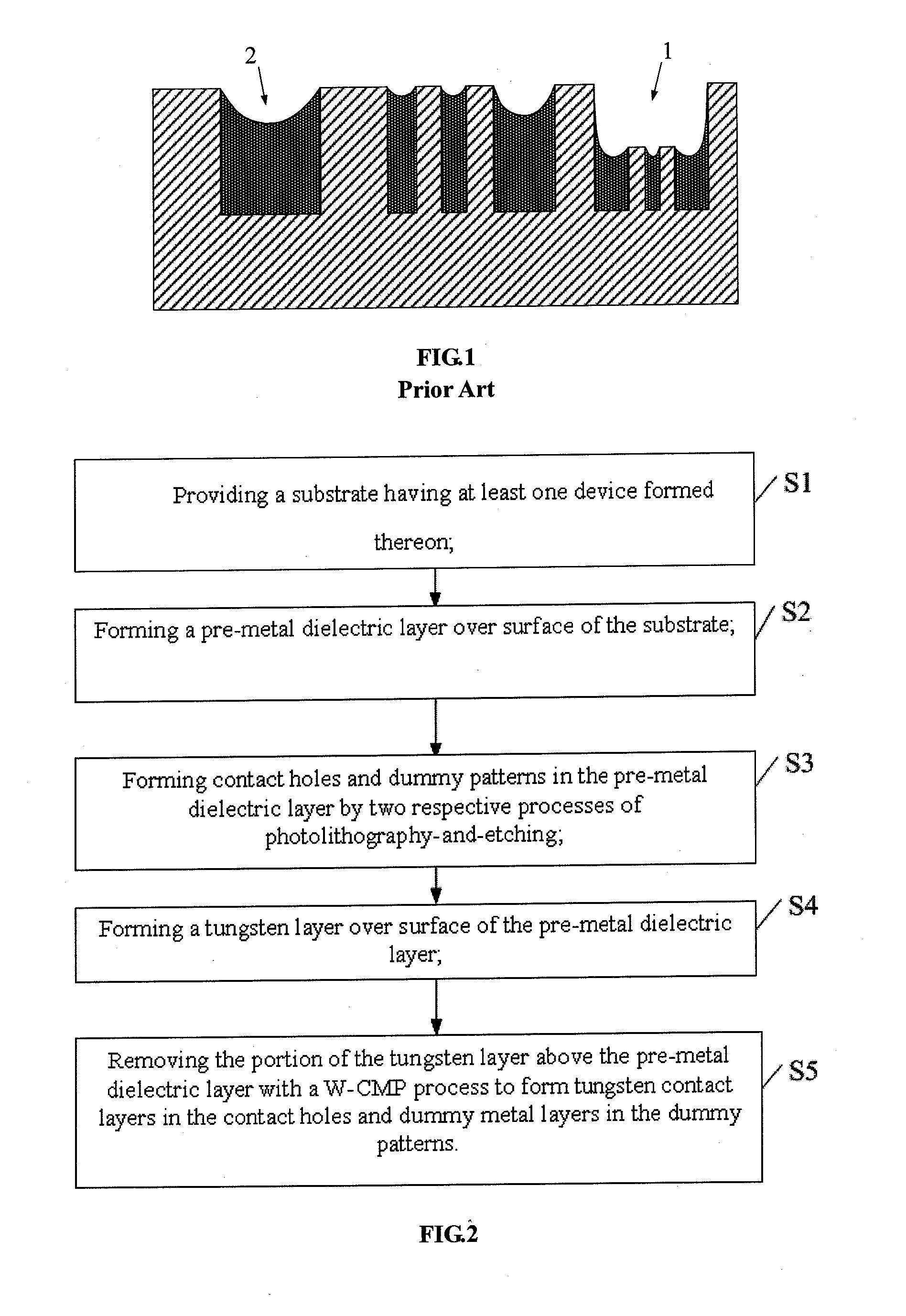
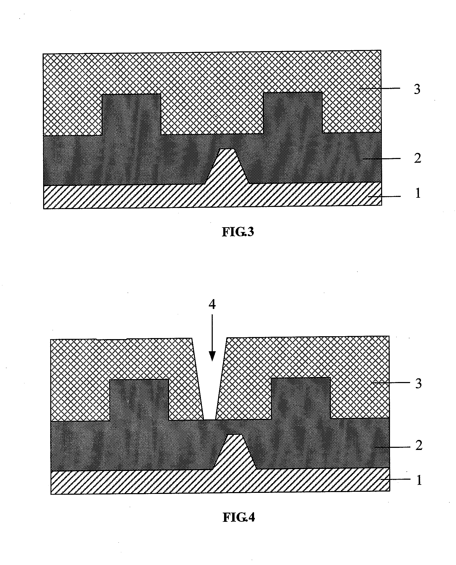
[0026]A contact hole layer which locates under a copper interconnection layer is generally formed by tungsten (W), and is generally planarized by using a W-CMP process. Similar to the Cu-CMP process, the surface planarity after W-CMP may be improved by inserting dummy patterns in the layout of the contact hole layer. However, if dummy patterns are formed simultaneously with contact holes by using one photolithography-and-etching process, this will lead to the formation of dummy patterns that have a same depth with that of the contact holes, meaning that the dummy patterns formed will also be through the pre-metal dielectric (PMD) layer, thus creating a high possibility for metal filled in the dummy patterns to contact with gate electrodes and active-ar...


PUM


Abstract

A fabrication method for improving surface planarity after tungsten chemical mechanical polishing (W-CMP) is disclosed. The method forms contact holes and dummy patterns by performing two respective photolithography-and-etching processes to ensure that the dummy patterns have a depth smaller than that of the contact holes. Then the method fills tungsten into the contact holes and dummy patterns and removes the redundant tungsten by a W-CMP process. With such a method, difference of wiring density between areas can be reduced by the dummy patterns, and hence a better surface planarity of the contact hole layer can be achieved. Besides, as the dummy patterns are formed in a pre-metal dielectric layer and their depth is well controlled, tungsten filled in the dummy patterns will not contact with the device area below the pre-metal dielectric layer, and thus will not affect the performance of the device.

Description

CROSS-REFERENCES TO RELATED APPLICATIONS[0001]This application claims the priority of Chinese patent application number 201210048734.8, filed on Feb. 28, 2012, the entire contents of which are incorporated herein by reference.TECHNICAL FIELD[0002]The present invention relates to microelectronics, and more particularly, to a fabrication method for improving surface planarity after tungsten chemical mechanical polishing (W-CMP).BACKGROUND[0003]With the development of very-large-scale integration (VLSI), the critical dimension of ICs continues to decrease and the integration of ICs continues to increase, back end interconnections generally adopt wirings with three-dimensional architectures and multiple layers. Meanwhile, copper (Cu) interconnection has many advantages incomparable with aluminum interconnection for the fabrication of ICs at 130 nm technology node and below, and has thus become the dominant interconnection process. Damascene process is indispensable in the realization of...

Claims


Application Information

Patent Timeline
IPC IPC(8): H01L21/768
CPCH01L21/3212H01L21/7684H01L23/522H01L2924/0002H01L2924/00
Inventor FANG, JINGXUNZHANG, CHUANMINZUO, WEITONG, XIAOGANGWANG, ZHEDENG, LEIWEN, JING
Owner SHANGHAI HUALI MICROELECTRONICS CORP
Why Eureka
Try Eureka