Organic el element

a technology of organic el and elements, applied in the field of organic el (electroluminescence) elements, to achieve the effect of easy extraction of substrates and easy optical designs

Inactive Publication Date: 2013-09-05
PANASONIC CORP
View PDF4 Cites 1 Cited by
  • Summary
  • Abstract
  • Description
  • Claims
  • Application Information

AI Technical Summary

Benefits of technology

[0008]The present invention is to solve the above problems, and an object of the present invention is to provide an organic EL element which has high luminous efficiency, has a long life, and has little change in chromaticity.

Problems solved by technology

Moreover, it is difficult for holes to reach an electron transport layer, so that the electron transport layer is not deteriorated, and the organic EL element can thereby have the long life.

Method used


Image

  • Organic el element
  • Organic el element

Examples


modification example

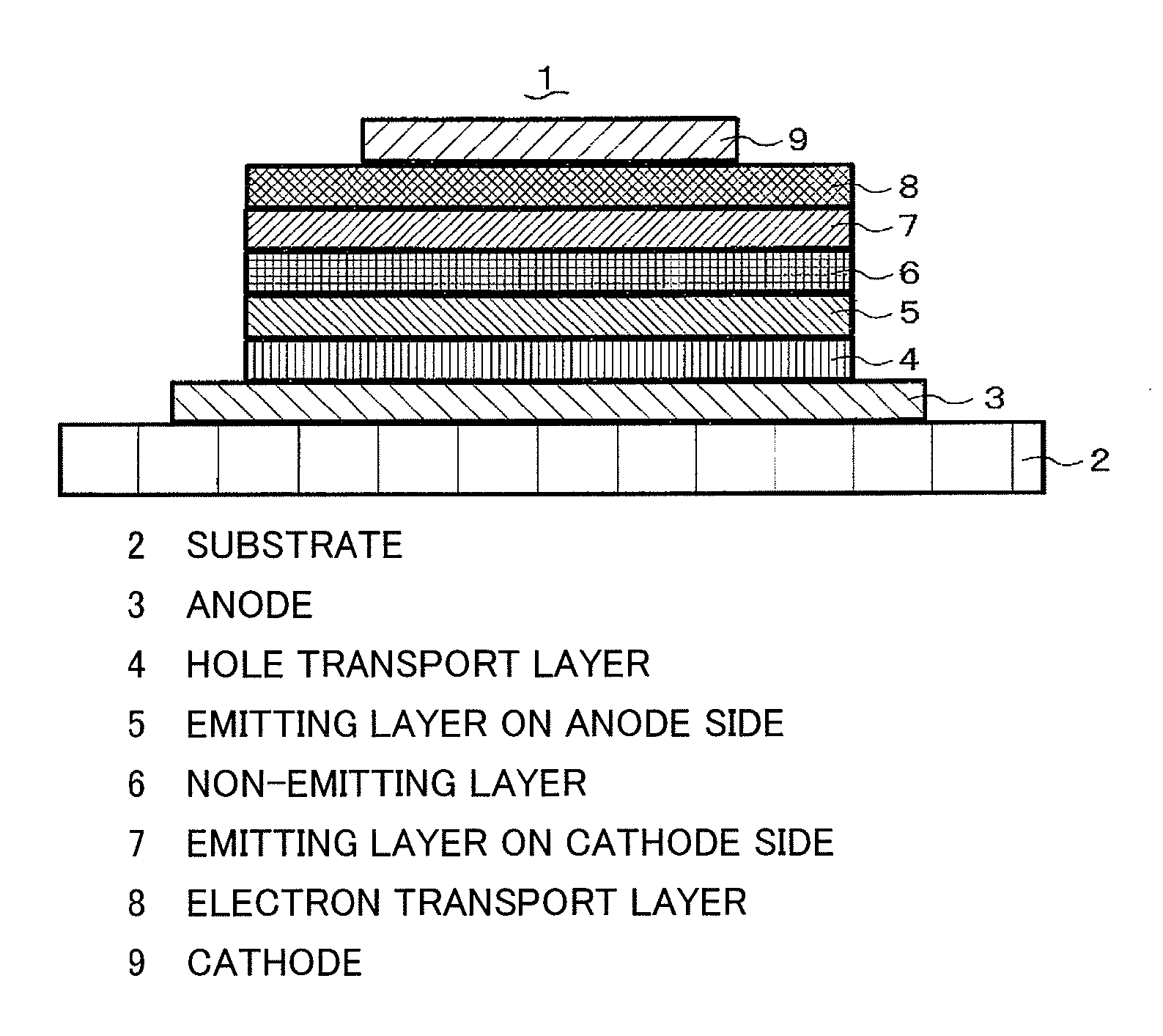
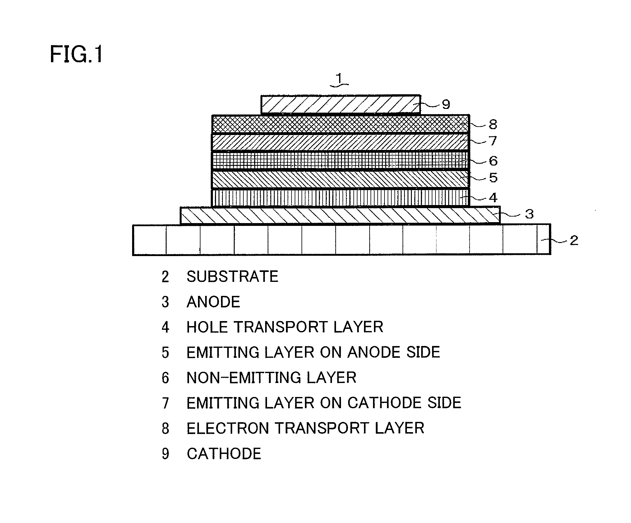
[0045]A modification example of the organic EL element 1 is described below. The organic EL element 1 of the modification example differs from that of the above preferred embodiment in that the non-emitting layer 6 has the electron transporting property instead of the hole transporting property and at least one energy transfer auxiliary material is included in the electron transporting material in the non-emitting layer 6. In the organic EL element 1, the energy transfer auxiliary material transfers the excitation energy in the non-emitting layer 6 to the emitting layers 5 and 7 adjacent to the non-emitting layer 6 effectively, so that the luminous efficiency of the emitting layers 5 and 7 can be enhanced. Moreover, due to the emitting layer 5 on the anode side which has the hole transporting property, it is difficult for the electrons to reach the hole transport layer 4, so that the hole transport layer 4 is not deteriorated, and the organic EL element 1 can thereby have the long l...

working example 1

[0050]The organic EL element 1 is formed by laminating, in order from the substrate 2 side, the anode 3, the hole transport layer 4, the emitting layer 5 on the anode side which is made of the host material and the emitting dopant, the non-emitting layer 6 which is made of the hole transporting material and the energy transfer auxiliary material, the emitting layer 7 on the cathode side which is made of the host material and the emitting dopant, the electron transport layer 8, and the cathode 9 on the substrate 2. Materials of the respective layers are as follows: the substrate 2 is made of alkali-free glass; the anode 3 is made of ITO; the hole transport layer 4 is made of NPD; the host material of the emitting layer 5 on the anode side is NPD; the emitting dopant of the emitting layer on the anode side is 2-methyl-6-[2-(2,3,6,7-tetrahydro-1H,5H-benzo[ij]quinolizin-9-yl)ethenyl]-4H-pyran-4-ylidene]propane-dinitrile (DCM2); the hole transporting material of the non-emitting layer 6 ...

working example 2

[0051]The organic EL element 1 is obtained in a manner similar to the working example 1 except that the energy transfer auxiliary material of the non-emitting layer 6 is ruburene.


PUM

PropertyMeasurementUnit
ionization potentialaaaaaaaaaa
thicknessaaaaaaaaaa
emission wavelengthaaaaaaaaaa

Abstract

Organic EL element is formed by laminating two emitting layers between an anode and a cathode with a hole transporting non-emitting layer interposed between the two emitting layers. Emitting layer on an anode side is a hole transporting emitting layer, emitting layer on a cathode side is an electron transporting emitting layer. Non-emitting layer includes at least one energy transfer auxiliary material in a hole transporting material. In the organic EL element, the energy transfer auxiliary material transfers excitation energy in the non-emitting layer to the emitting layers adjacent to the non-emitting layer effectively, so that luminous efficiency of the emitting layers can be enhanced. It is difficult for holes to reach an electron transport layer so that the electron transport layer is not deteriorated, and the organic EL element can have a long life.

Description

CROSS-REFERENCE TO RELATED APPLICATIONS[0001]The present application is a divisional of U.S. application Ser. No. 13 / 259,208, which is a National Stage of International Patent Application No. PCT / JP2010 / 054700, filed Mar. 18, 2010 which claims priority to Japanese Application No. JP 2009-074783 filed Mar. 25, 2009. The disclosures of application Ser. Nos. 13 / 259,208 and PCT / JP2010 / 054700 are expressly incorporated by reference herein in their entireties.TECHNICAL FIELD[0002]The present invention relates to an organic EL (electroluminescence) element which is used for a flat panel display, a backlight for a liquid crystal display, an illumination light source, etc.BACKGROUND ART[0003]An organic EL element has received attention in recent years by reason that a high-brightness flat emission can be achieved by a low voltage of several volts. The organic EL element includes an anode, an emitting layer, and a cathode, and the anode injects holes into the emitting layer and the cathode in...

Claims


Application Information

Patent Timeline
Patent Type & Authority Applications(United States)
IPC IPC(8): H01L51/50
CPCH01L51/508H01L51/5044H10K50/131H10K50/166H10K50/15
Inventor SASAKI, HIROYUKI
Owner PANASONIC CORP
Why Eureka
Try Eureka