Semiconductor storage device having nonvolatile semiconductor memory

a semiconductor memory and non-volatile technology, applied in the direction of electric digital data processing, instruments, computing, etc., can solve the problems of increasing the probability of data being lost, data being overwhelmed, data being lost, etc., to prevent a specific block from becoming unusable, and the level of deterioration will differ by block.

Active Publication Date: 2013-09-12
HITACHI LTD
View PDF5 Cites 69 Cited by
  • Summary
  • Abstract
  • Description
  • Claims
  • Application Information

AI Technical Summary

Benefits of technology

[0013]For this reason, the SSD performs control (called wear leveling) to equalize the number of erases for each block of the flash memory for the purpose of preventing a specific block from becoming unusable due to a concentration of rewrit

Problems solved by technology

For this reason, fail bits (a bit associated with a cell for which the state was erroneously determined to be different), which are included in read data from a flash memory, have increased in recent years, increasing the likelihood of the correction capabilities of the correction codes assigned to data being overwhelmed and data being lost.
When a read parameter is inappropr

Method used


Image

  • Semiconductor storage device having nonvolatile semiconductor memory
  • Semiconductor storage device having nonvolatile semiconductor memory
  • Semiconductor storage device having nonvolatile semiconductor memory

Examples


example 1

[0045]First, a computer system related to Example 1 will be explained.

(1-1) Computer System Configuration

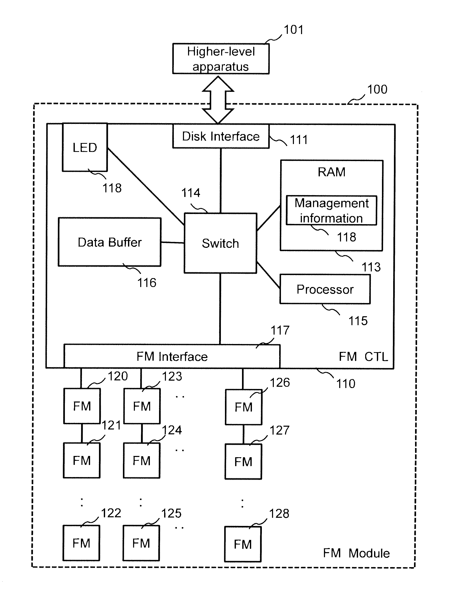
[0046]FIG. 1 is a detailed block diagram of a computer system related to Example 1.

[0047]A flash memory module 100, which serves as an example of a semiconductor storage device in the computer system, is coupled to a higher-level apparatus 101.

[0048]The higher-level apparatus 101, for example, is equivalent to a computer or a file server, which forms the core of a business system, or a storage system to which a large number of storage apparatuses are coupled. The higher-level apparatus 101 comprises hardware resources, such as a processor, a memory, a network interface, and a local input / output device(s), and comprises software resources, such as a device driver(s), an operating system (OS), and an application program(s). The higher-level apparatus 101 communicates with the flash memory module 100 and performs read / write requests with respect to the flash memory module 100 in acc...

example 2

[0141]Next, a computer system related to Example 2 will be explained.

[0142]In Example 1, an example is given in which, when the flash memory module 100 receives a read request from the higher-level apparatus 101, the number of times a read is re-executed is reduced in accordance with acquiring an appropriate read parameter based on the attribute information (temperature, number of erases, and elapsed time since data recorded) of the read-target area of this read request, and reading the data from the FM chip using this read parameter.

[0143]In contrast to this, in Example 2, a check is performed with respect to each storage area of the flash memory module 100 at a timing (for example, regularly), which differs from a read request by the higher-level apparatus 101, and a read parameter, which actually makes a read possible for each storage area, is identified beforehand. Then, when there is a read request from the higher-level apparatus 101, a read is executed using the pre-identified...

example 3

[0199]FIG. 20 is detailed block diagram showing an example of a computer system related to Example 3.

[0200]The computer system comprises a storage system 10 and a host computer (host) 20. There can be one or more storage systems 10 and hosts 20, respectively. The storage system 10 and the host 20 are coupled to one another via a communication network (for example, a SAN (Storage Area Network)). The storage system 10 stores data, which is used in the host 20. The host 20 executes various processes, reads data from the storage system 10, and writes data to the storage system 10.

[0201]The storage system 10 comprises multiple storage devices, and a RAID (abbreviation for a Redundant Array of Independent (or Inexpensive) Disks) controller device 30, which is coupled to the multiple storage devices.

[0202]The multiple storage devices comprise multiple types of storage devices. One or more of at least one type of storage device may exist. As the storage devices, for example, there are a fla...


PUM


Abstract

A semiconductor storage device has a nonvolatile semiconductor memory comprised from multiple storage areas, and a controller, which is coupled to the nonvolatile semiconductor memory. The controller (A) identifies a storage area state, which is the state of a storage area, (B) decides, based on the storage area state identified in the (A), a read parameter, which is a parameter for use when reading data from a storage area with respect to a storage area of this storage area state, and (C) uses the read parameter decided in the (B) with respect to a read-target storage area and reads data from this read-target storage area.

Description

TECHNICAL FIELD[0001]The present invention relates to reading data from an electrically rewritable nonvolatile semiconductor memory.BACKGROUND ART[0002]Flash memory is generally well-known as an example of a nonvolatile semiconductor memory. One example of a semiconductor storage device comprising flash memory is the SSD (Solid State Drive). An SSD is advantageous compared to a HDD (Hard Disk Drive) in that it features higher read and write processing performance.[0003]A flash memory comprises multiple cells, and a single cell, for example, maintains two states over time. More specifically, digital data is recorded by associating one of the two states of the cell with the bit value “1”, and the other of the two states with the bit value “0”. For example, in the case of a SLC (Single Level Cell) type flash memory, which is an example of a semiconductor recording element, digital data is recorded by associating a state in which an electron is injected onto a FG (Floating Gate) of the ...

Claims


Application Information

Patent Timeline
IPC IPC(8): G06F12/00
CPCG11C16/00G11C16/3431G11C29/028G11C29/021G11C16/3495G06F3/0616G06F3/0629G06F3/0679
Inventor SUZUKI, AKIFUMITSUNEHIRO, TAKASHI
Owner HITACHI LTD
Why Eureka
Try Eureka