Semiconductor memory device

a memory device and semiconductor technology, applied in the field of semiconductor memory devices, can solve the problems of failure to eliminate the probability of information loss, failure to avoid the loss of information stored in the selected memory cell, and the reliability of data storage will be declined, so as to achieve the effect of reducing production costs and simplifying the semiconductor memory devi

Active Publication Date: 2009-03-31
SAMSUNG ELECTRONICS CO LTD
View PDF8 Cites 16 Cited by
  • Summary
  • Abstract
  • Description
  • Claims
  • Application Information

AI Technical Summary

Benefits of technology

[0029]According to the semiconductor memory device of the seventh feature, the select transistor in the memory cell and the transistor constituting the peripheral circuit can be ...

Problems solved by technology

However, the semiconductor memory device described above is contemplated for inhibiting the loss of information stored in the memory cells not to be read during the reading action on the selected memory cell to be read but fails to avoid the loss of information stored in the selected memory cell to be read.
Accordingly, when the selected memory cell to be read is repeatedly subjected to the reading action a number of times, its stored information may be lost due to a change in the re...

Method used


Image

  • Semiconductor memory device
  • Semiconductor memory device
  • Semiconductor memory device

Examples


first embodiment

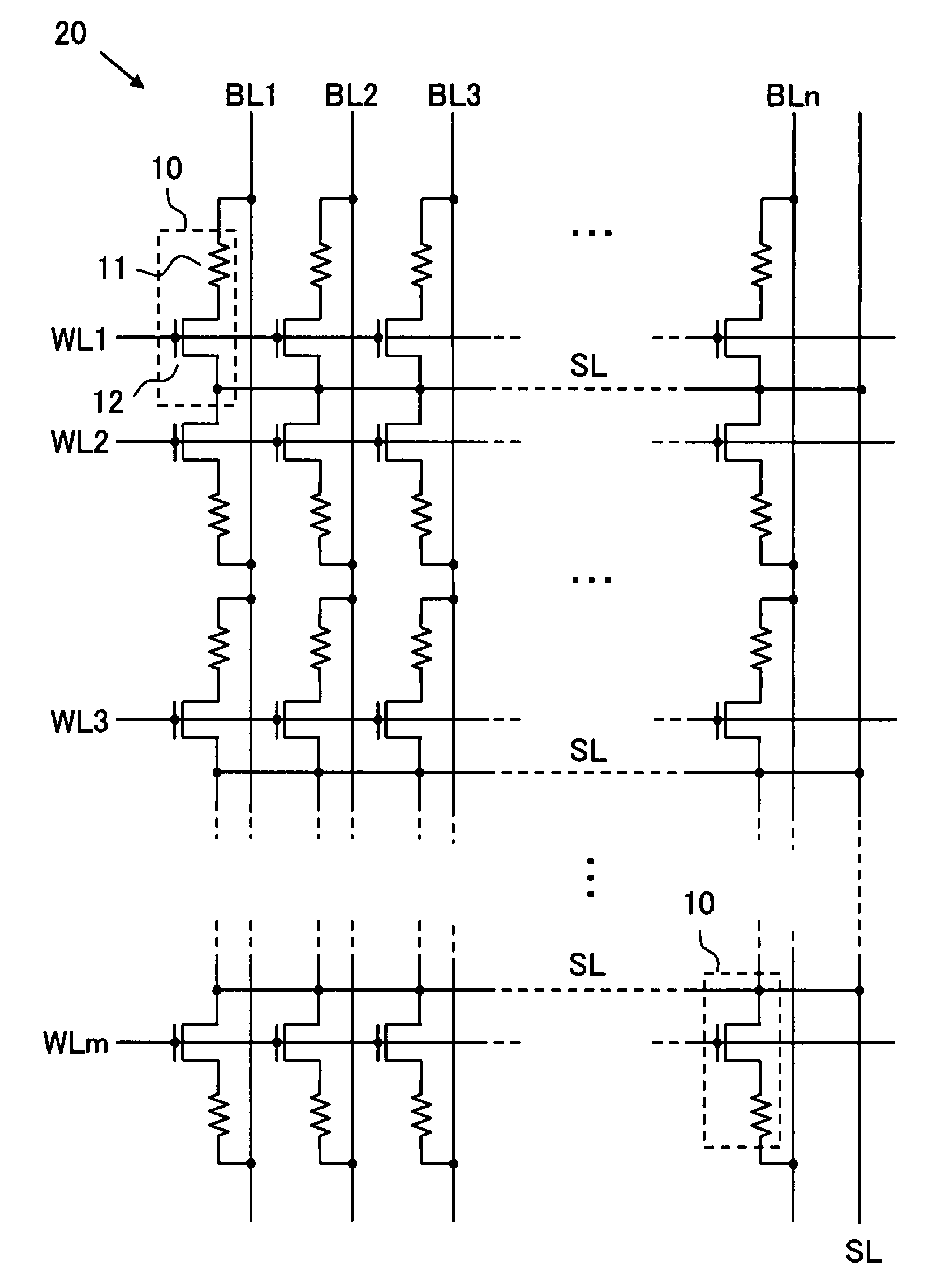
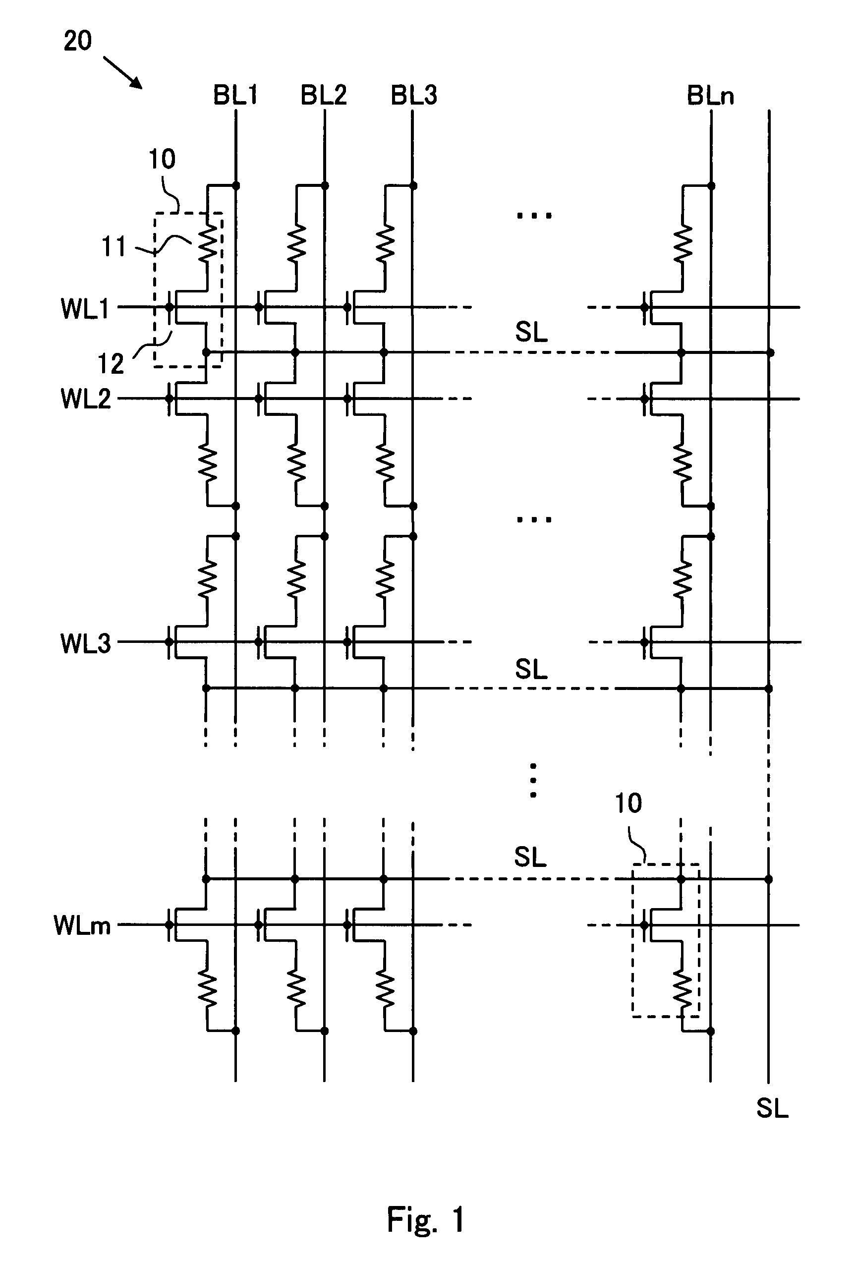
[0054]The inventive device of this embodiment comprises, as shown in FIG. 1, one or more memory cell arrays 20 where a number of memory cells 10 are arranged in rows and columns and groups of words lines WL1 to WLm and bit lines BL1 to BLn arranged to extend along the rows and the columns respectively for selectively driving one or more of the memory cells of interest while a group of source lines SL is arranged to extend along the rows. Although the source lines SL extend along the rows in parallel to the word lines WL1 to WLm, each source line in each row, and are connected commonly at the outside of the memory cell array 20 in the embodiment shown in FIG. 1, they may be modified to one source line SL provided commonly for two adjacent word lines or may extend along the columns but not the rows. Alternatively, each memory cell array 20 may be accompanied with two or more of the source lines SL for selectively driving one or more of the memory cells of interest in cooperation with ...

second embodiment

[0090]The second embodiment of the present invention will be described. The inventive device of the second embodiment comprises, as shown in FIG. 13, one or more memory cell arrays 40 where a number of memory cells 16 are arranged in rows and columns and groups of words lines WL1 to WLm and bit lines BL1 to BLn arranged to extend along the rows and the columns respectively for selectively driving one or more of the memory cells of interest while a group of source lines SL is arranged to extend along the rows. Although the source lines SL extend along the rows in parallel to the word lines WL1 to WLm, each source line in each row, and are connected commonly at the outside of the memory cell array 40 in the embodiment shown in FIG. 13, they may be modified to one source line SL provided commonly for two adjacent word lines or may extend along the columns but not the rows. Alternatively, each memory cell array 40 may be accompanied with two or more of the source lines SL for selectivel...


PUM


Abstract

The possibility of the loss of information stored in a memory cell which is caused by repeating the reading action on the same memory cell comprising a variable resistance element and a select transistor can significantly be reduced. A voltage applying circuit for selecting one or more of the memory cells from a memory cell array and applying voltages to the word lines, bit lines, and source lines for programming, erasing, and reading information applies a voltage between the bit line and the source line connected to the selected memory cell so that the voltage applied between the two ports of the variable resistance element in the selected memory cell during the reading action is equal in the polarity to one of the voltages applied between the two ports of the variable resistance element for the programming action and the erasing action respectively whichever is greater in the absolute value.

Description

CROSS REFERENCE TO RELATED APPLICATION[0001]This Nonprovisional application claims priority under 35 U.S.C. §119(a) on Patent Application No. 2006-208345 filed in Japan on 31 Jul., 2006 the entire contents of which are hereby incorporated by reference.BACKGROUND OF THE INVENTION[0002]1. Field of the Invention[0003]The present invention relates to a semiconductor memory device provided with a memory cell including a variable resistance element having two terminals, that can store information by varying its electric resistan ce between a first state and a second state when voltage having different polarities are separately applied to both ends thereof, and a select transistor whose source or drain is connected to one end of the variable resistance element.[0004]2. Description of the Related Art[0005]Nonvolatile semiconductor memory devices including typically flash memories have widely been marketed for use in computers, communications apparatuses, measuring apparatuses, automatic con...

Claims


Application Information

Patent Timeline
IPC IPC(8): G11C11/00
CPCG11C13/0007G11C13/0069G11C2013/009G11C2213/31G11C2213/34G11C2213/79
Inventor HORII, SHINJIYAMAGATA, SATORU
Owner SAMSUNG ELECTRONICS CO LTD
Why Eureka
Try Eureka