Light-Emitting Device and Manufacturing Method Thereof

Inactive Publication Date: 2013-09-19
SEMICON ENERGY LAB CO LTD
View PDF3 Cites 22 Cited by
  • Summary
  • Abstract
  • Description
  • Claims
  • Application Information

AI Technical Summary

Benefits of technology

[0048]According to the present invention, a light-emitting device in which voltage drop is suppressed and the light extraction efficiency is increased can

Problems solved by technology

If the voltage drop becomes marked, there is a problem that luminance cannot be obtained uniformly in the light-emitting region.
However, there is also a problem that an oxide conductor often used as a light-transmitting conductive material has relatively high resistivity.
An oxide film can be formed typically by a sputtering method; however,

Method used


Image

  • Light-Emitting Device and Manufacturing Method Thereof
  • Light-Emitting Device and Manufacturing Method Thereof
  • Light-Emitting Device and Manufacturing Method Thereof

Examples


embodiment 1

[0059]In this embodiment, a structure example of a light-emitting device according to one embodiment of the present invention and an example of a manufacturing method thereof will be described with reference to drawings.

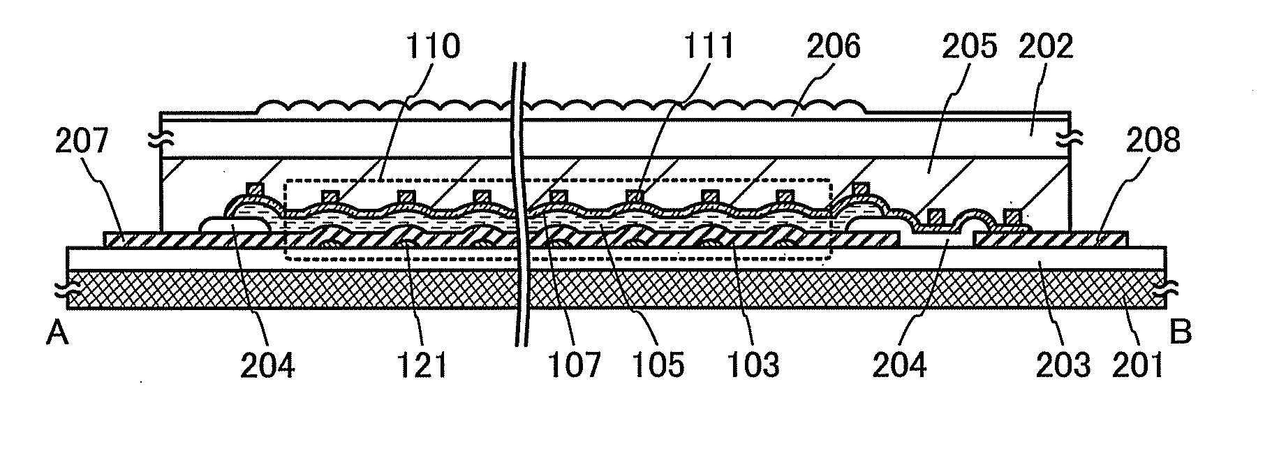
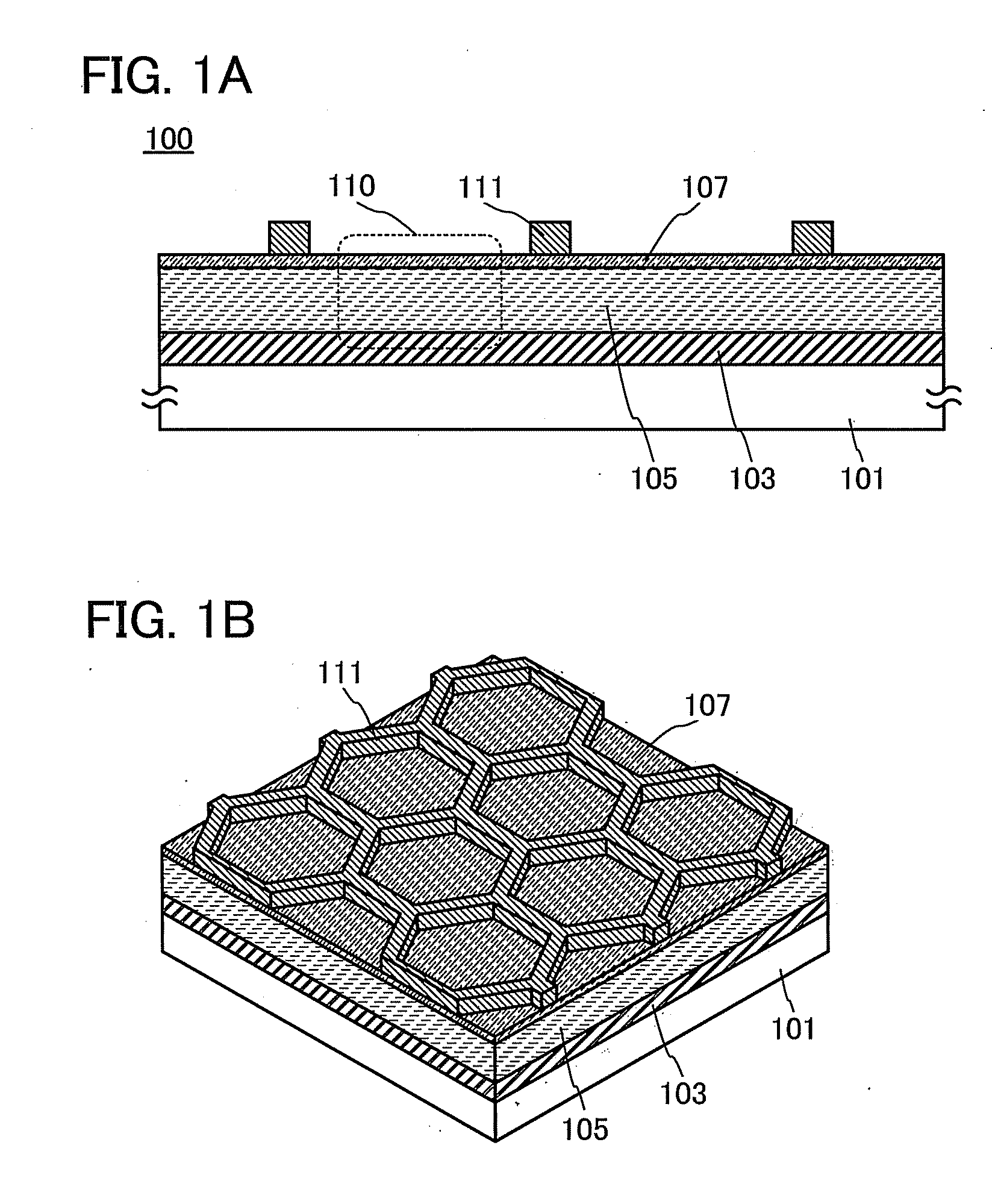
[0060]A schematic cross-section of a light-emitting device 100 which is one embodiment of the present invention is illustrated in FIG. 1A.

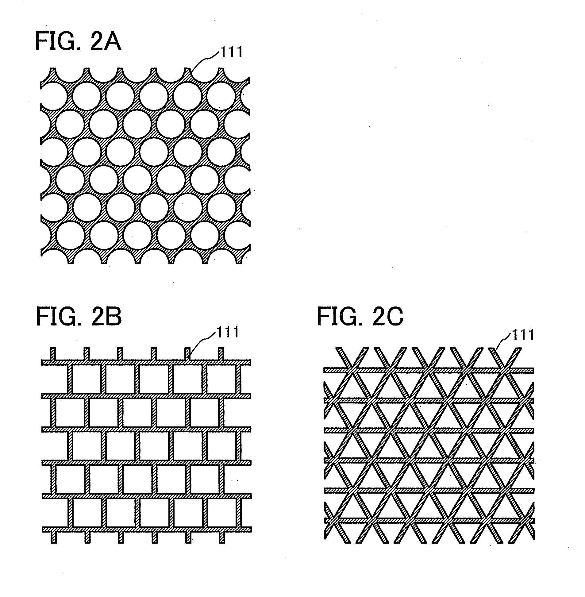
[0061]The light-emitting device 100 includes a light-emitting element 110 in which a first electrode layer 103, an EL layer 105, and a second electrode layer 107 are stacked in this order over a first substrate 101 having an insulating surface. Further, an auxiliary wiring 111 is provided on and in contact with the second electrode layer 107.

[0062]The first electrode layer 103 has reflective properties with respect to light emitted from the EL layer 105. The second electrode layer 107 has light-transmitting properties with respect to the light. Thus, the light-emitting element 110 is a top-emission type light-emitting element which...

embodiment 2

[0112]In this embodiment, a structure example of a light-emitting device which is different from the structure in the above embodiment is described with reference to drawings. Note that description of, the same portions as those in the above embodiment is skipped or simplified below.

[0113]FIG. 4A is a schematic cross-sectional view of a light-emitting device 120 exemplified in this structure example.

[0114]The light-emitting device 120 is different from the light-emitting device 100 in the above embodiment in that an auxiliary wiring 121 (also referred to as second auxiliary wiring) overlapping with the auxiliary wiring 111, when seen from the direction perpendicular to the insulating surface of the first substrate 101, is provided between the first electrode layer 103 and the first substrate 101.

[0115]The conductive material similar to that used for the auxiliary wiring 111 can be used for the auxiliary wiring 121.

[0116]The first electrode layer 103 is provided to cover the auxiliar...

modification example

[0132]A light-emitting device whose structure is different from the above structure example is described below.

[0133]FIG. 5 is a schematic cross-sectional view of a light-emitting device 140 described in this modification example. A difference between the light-emitting device 140 and the light-emitting device 120 is in that the light-emitting device 140 includes an insulating layer 125 with projections and depressions instead of the auxiliary wiring 121.

[0134]The upper surface of the insulating layer 125 which is in contact with the first electrode layer 103 has projections and depressions. The upper surface of the first electrode layer 103 has projections and depressions reflecting the shape of the insulating layer 125.

[0135]Thus, the upper surface of the first electrode layer 103 has projections and depressions also in a region not overlapping with the auxiliary wiring 111; thus, the ratio of the diffusely-reflected light to the whole light emitted from the EL layer 105 can be in...


PUM


Abstract

Provided is a light-emitting device in which a voltage drop is suppressed and light extraction efficiency is increased. Provided is a light-emitting device with increased productivity. Provided is a light-emitting device with high reliability. An extremely thin conductive film from 3 nm to 50 nm is used as an electrode on a light-emitting side and an auxiliary wiring is provided in contact with the electrode. When the width of the auxiliary wiring is 100 μm or less, the auxiliary wiring is hardly perceived with the naked eye, so that a light-emitting device in which light extraction efficiency is increased and luminance is obtained uniformly. The extremely thin auxiliary wiring can be formed by nanoimprinting technology. With use of nanoimprinting technology, the width of the auxiliary wiring can be reduced to 10 nm or less.

Description

BACKGROUND OF THE INVENTION[0001]1. Field of the Invention[0002]The present invention relates to a light-emitting device including an organic EL element.[0003]2. Description of the Related Art[0004]Research and development of organic EL (ElectroLuminescent) elements have been extensively conducted. The fundamental structure of the organic EL element is that a layer containing a light-emitting organic compound is sandwiched between a pair of electrodes. By applying voltage to this element, light emission from the light-emitting organic compound can be obtained.[0005]Organic EL elements can be formed in the form of a film and thus can easily constitute large-area elements, and also have great potential as planar light sources applicable to lighting and the like.[0006]For example, a lighting device including an organic EL element is disclosed in Patent Document 1.[0007]In addition, as for an organic EL element, there are a top-emission type in which light is extracted from the side of ...

Claims


Application Information

Patent Timeline
IPC IPC(8): H01L51/52
CPCH01L51/5271H01L51/5275H01L51/5209H01L51/5212H01L51/5228H01L51/0022H01L51/5225H10K71/611H10K50/813H10K50/814H10K50/822H10K50/824H10K50/858H10K50/856
Inventor YAMAZAKI, SHUNPEI
Owner SEMICON ENERGY LAB CO LTD
Why Eureka
Try Eureka