Hybrid Energy Storage Devices

a technology of energy storage devices and hybrids, applied in the direction of electrochemical generators, cell components, transportation and packaging, etc., can solve the problem of significant limitation of the lifetime of si anodes

Inactive Publication Date: 2013-09-19
CF TRAVERSE LLC
View PDF4 Cites 32 Cited by
  • Summary
  • Abstract
  • Description
  • Claims
  • Application Information

AI Technical Summary

Benefits of technology

[0025]Various embodiments of the invention include a system comprising: means for establishing a potential gradient at an anode of a charge storage device, the anode including an electrolyte, a plurality of surface effect dominant sites, an intercalation material and a substrate; means for receiving a charge carrier of the electrolyte at one of the surface effect dominant sites; means for receiving an electron at the charge carrier from one of the surface effect dominant sites; and means for receiving a charge carrier at the intercalation material.
[0026]Various embodiments of the invention include a method of producing an energy storage device, the method comprising: providing a conductive substrate; growing support filaments on the substrate; applying intercalation material to the support nanofibers, the intercalation material being configured for intercalation of charge carriers; and applying a plurality of surface effect dominant sites in close proximity to the intercalation material.
[0027]Various embodiments of the invention include a method of producing an anode, the method comprising: providing a conductive substrate; mixing a binding material, surface effect dominant sites and intercalation material, the surface effect dominant sites being configured to accept electrons from charge carriers at a first reaction potential and the intercalation material being configured to accept the charge carriers or electrons from the charge carriers at a second reaction potential; and applying the binding material, surface effect dominant sites and intercalation material to the substrate.
[0028]Various embodiments of the invention include a method of producing an energy storage device, the method comprising: providing a conductive substrate; providing support filaments; applying intercalation material to the support filaments, the intercalation material being configured for intercalation of charge carriers; and adding surface effect dominant sites to the support filaments.
[0029]Various embodiments of the invention include a method of charging a charge storage device, the method comprising establishing a potential between a cathode and an anode of the charge storage device, the charge storage device including an electrolyte; receiving a first charge carrier of the electrolyte at a surface effect dominant site of the anode; transferring an electron of the anode to the first charge carrier; receiving a second charge carrier of the electrolyte at an intercalation material of the anode; and transferring an electron from the intercalation material to the second charge carrier.
[0030]Various embodiments of the invention include a method of charging a charge storage device, the method comprising: establishing a potential gradient at an anode of the charge storage device, the anode including an electrolyte, a plurality of nanoparticles having surface effect dominant sites, an intercalation material and a substrate; receiving a first charge carrier of the electrolyte at one of the surface effect dominant sites; transferring an electron to the first charge carrier from the one of the surface effect dominant sites; receiving a second charge carrier at the intercalation material of the anode; and transferring an electron from the intercalation material to the second charge carrier.

Problems solved by technology

However, the large volume expansion of lithiated Si by up to ˜300% causes great structural stress that in the past inevitably lead to fractures and mechanical failure, which significantly limited the lifetime of Si anodes.

Method used


Image

  • Hybrid Energy Storage Devices
  • Hybrid Energy Storage Devices
  • Hybrid Energy Storage Devices

Examples


Embodiment Construction

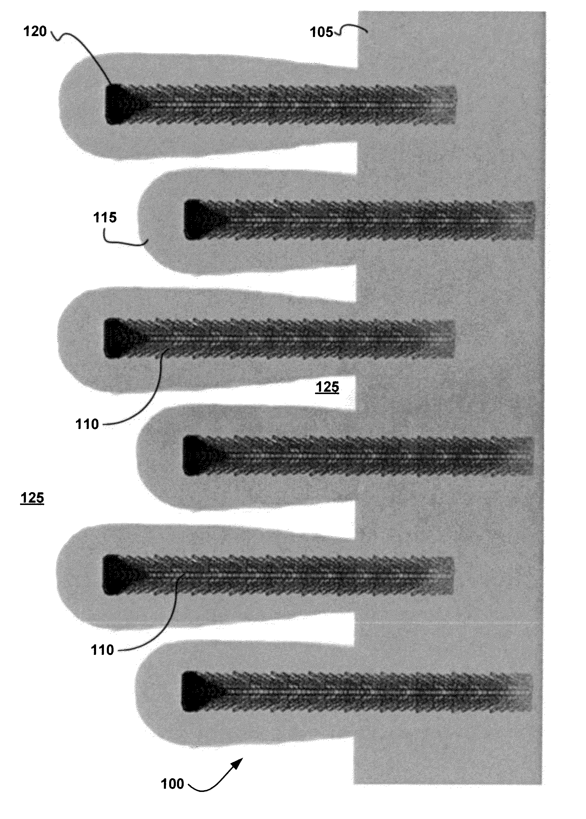
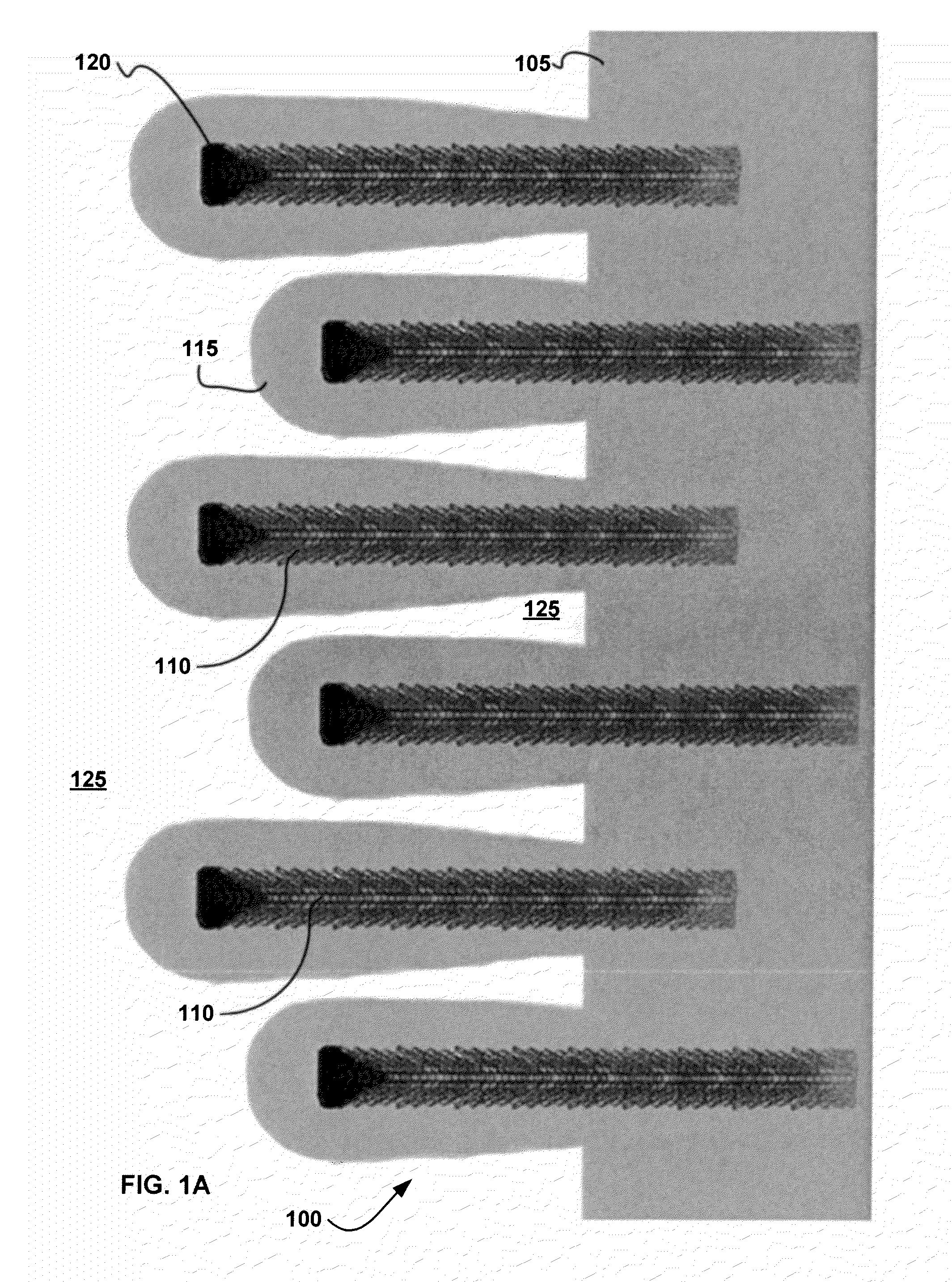
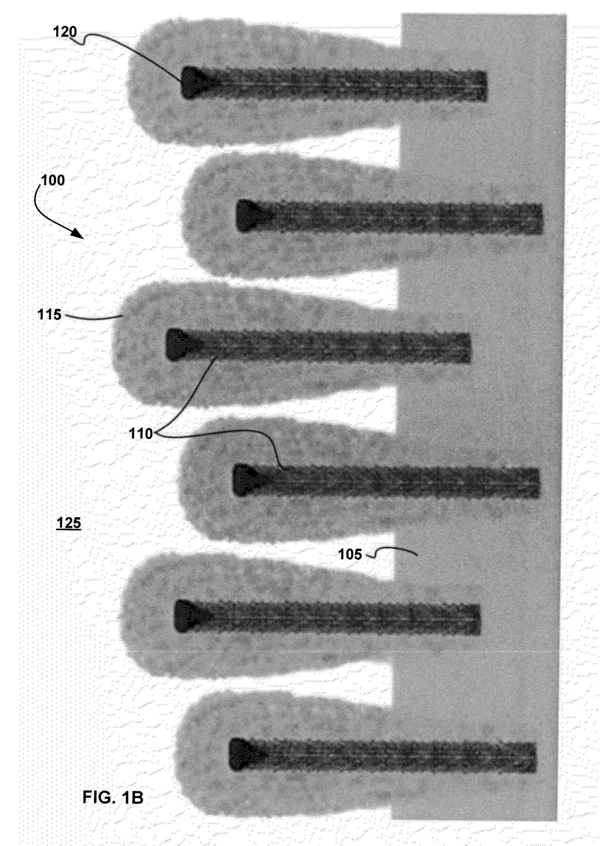
[0055]FIGS. 1A and 1B illustrate a CNF Array 100 comprising a plurality of CNF 110 grown on a conductive Substrate 105, according to various embodiments of the invention. In FIG. 1A the CNF Array 100 is shown in the Li extracted (discharged) state and in FIG. 1B the CNF Array 100 is shown in the Li inserted (charged) state. The CNF 110 in these and other embodiments discussed herein are optionally vertically aligned. The CNF 110 are grown on a Substrate 105 of Cu using a DC-biased plasma chemical vapor deposition (PECVD) process. As discussed above, the CNFs 110 grown by this method can have a unique morphology that includes a stack of conical graphitic structures similar to stacked cups or cones or a spiral. This creates a very fine structure that facilitates lithium intercalation. This structure is referred to here as the “stacked-cone”structure elsewhere herein. In larger length scale, these CNFs 110 are typically uniformly aligned normal to the substrate surface and are well sep...


PUM

PropertyMeasurementUnit
lengthaaaaaaaaaa
lengthaaaaaaaaaa
diametersaaaaaaaaaa

Abstract

A novel hybrid lithium-ion anode material based on coaxially coated Si shells on vertically aligned carbon nanofiber (CNF) arrays. The unique cup-stacking graphitic microstructure makes the bare vertically aligned CNF array an effective Li+ intercalation medium. Highly reversible Li+ intercalation and extraction were observed at high power rates. More importantly, the highly conductive and mechanically stable CNF core optionally supports a coaxially coated amorphous Si shell which has much higher theoretical specific capacity by forming fully lithiated alloy. Addition of surface effect dominant sites in close proximity to the intercalation medium results in a hybrid device that includes advantages of both batteries and capacitors.

Description

CROSS-REFERENCE TO RELATED APPLICATIONS[0001]This application is:[0002]a continuation of U.S. non-provisional patent application Ser. No. 13 / 779,409 filed Feb. 27, 2013;[0003]a continuation-in-part of U.S. non-provisional patent application Ser. No. 13 / 725,969 filed Dec. 21, 2012 which claimed priority to U.S. provisional patent applications 61 / 578,545 filed Dec. 21, 2011, 61 / 603,833 filed Feb. 27, 2012 and 61 / 615,179 filed Mar. 23, 2012, and which in turn is a continuation-in-part of U.S. non-provisional patent application Ser. No. 12 / 392,525 filed Feb. 25, 2009 now U.S. Pat. No. 8,420,258;[0004]a continuation-in-part of U.S. non-provisional patent application Ser. No. 12 / 904,113 filed Oct. 13, 2010 which in turn claims benefit and priority to U.S. provisional patent application 61 / 254,090 filed Oct. 22, 2009;[0005]and claims benefit and priority to U.S. provisional patent applications:[0006]61 / 667,876 filed Jul. 3, 2012,[0007]61 / 677,317 filed Jul. 30, 2012, and[0008]61 / 752,437 fil...

Claims


Application Information

Patent Timeline
Patent Type & Authority Applications(United States)
IPC IPC(8): H01M4/134H01M4/66
CPCY02E60/122H01G11/50H01M4/131H01M4/133H01M4/139H01M4/70H01M10/0525H01M4/134H01M4/661Y02T10/7011Y02T10/7022Y02E60/13H01G11/24H01G11/36B82Y30/00Y02T10/70Y02E60/10
Inventor ROJESKI, RONALD A.
Owner CF TRAVERSE LLC
Why Eureka
Try Eureka