Semiconductor testing apparatus

Inactive Publication Date: 2013-10-03
SEMICONTEST
View PDF9 Cites 4 Cited by
  • Summary
  • Abstract
  • Description
  • Claims
  • Application Information

AI Technical Summary

Benefits of technology

[0027]According to such a configuration of the present disclosure, unlike conventional methods, components are mounted on an upper side of a testing apparatus PCB, with the mechanical design structure of the test socket changed so as to prevent mechanical interference with the components mounted thereon. Accordingly, it is possible to mount the components that must be placed most closely on an upper side of the testing apparatus PCB thereon, innovatively improving the semiconductor testing environment.
[0028]Meanwhile, a middle PCB is provided between a test object and a testing apparatus PCB. This has an effe

Problems solved by technology

A problem of the design structure of FIG. 2 is that the path between the via hole 32 that is connected to the test socket 140 and the capacitor 36 is too long.
Furthermore, due to the existence of the unnecessary via hole 37 perforated to the opposite side of the test object 152, an unwanted inductance exists, causing degradation of PI (Power Integrity) and performance.
A problem of the design structure of FIG. 3 is that the capacitor 36 is mounted on the bottom surface

Method used


Image

  • Semiconductor testing apparatus
  • Semiconductor testing apparatus
  • Semiconductor testing apparatus

Examples


Example

First Exemplary Embodiment

[0050]FIG. 5 is a view for explaining a main configuration of a semiconductor testing apparatus in accordance with a first exemplary embodiment of the present disclosure.

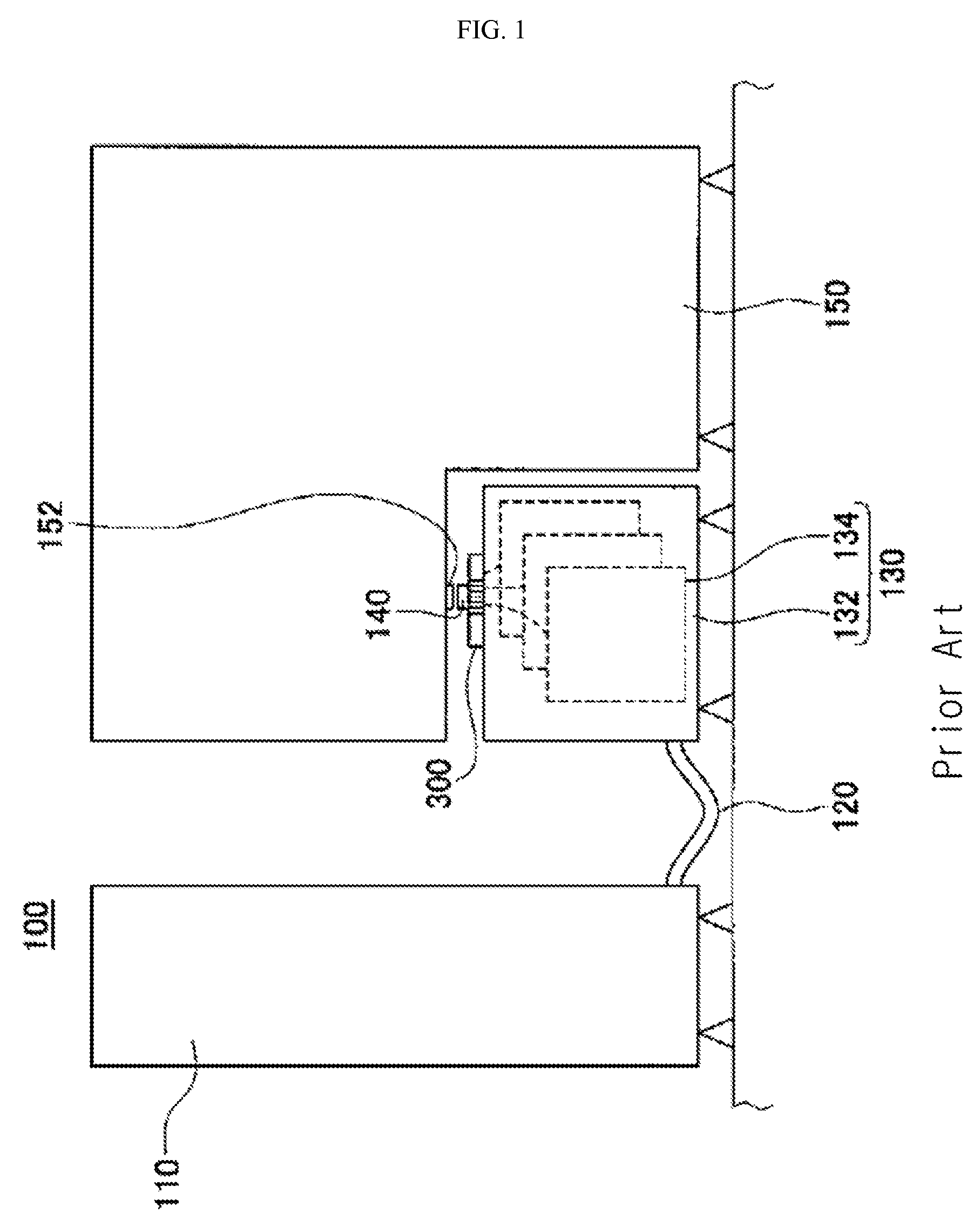
[0051]The semiconductor testing apparatus of the first exemplary embodiment includes a printed circuit board 300, and a test socket 140 mounted on an upper surface of the printed circuit board 300.

[0052]The test socket 140 forms a signal connection path for a test object 152(semiconductor) and the printed circuit board 300. The test socket 140 has one or more conductive material tracks 21 that transfer signals between the test object 152 and the printed circuit board 300. Herein, any type of conductive material track 21 may be used as long as it has an electricity transfer path between a bottom surface and upper surface of a socket such as a Rubber Socket Type or Pogo Type etc.

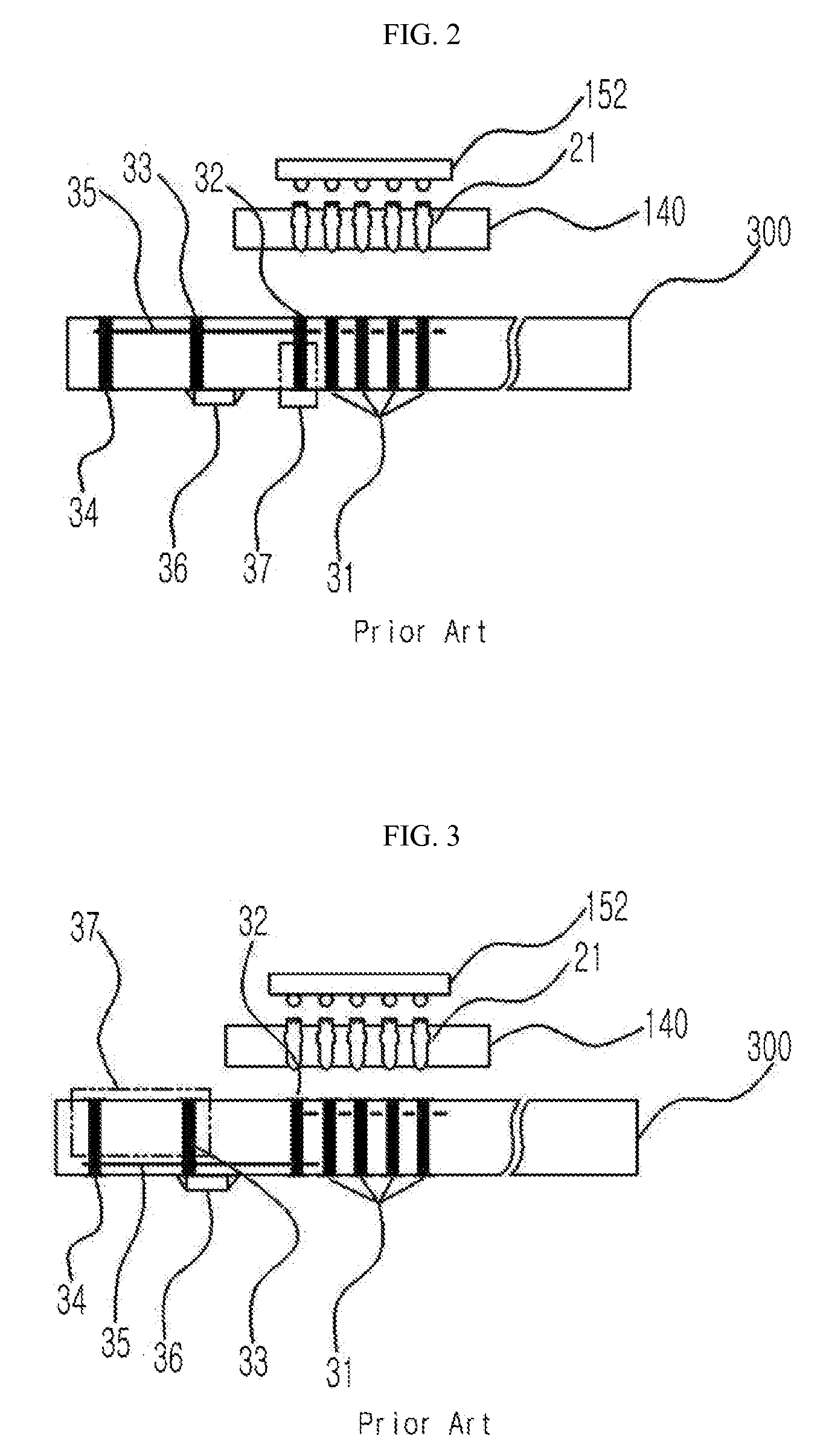
[0053]In a conventional testing apparatus PCB, a chip shaped capacitor 36 is located on a bottom surface of a print...

Example

Second Exemplary Embodiment

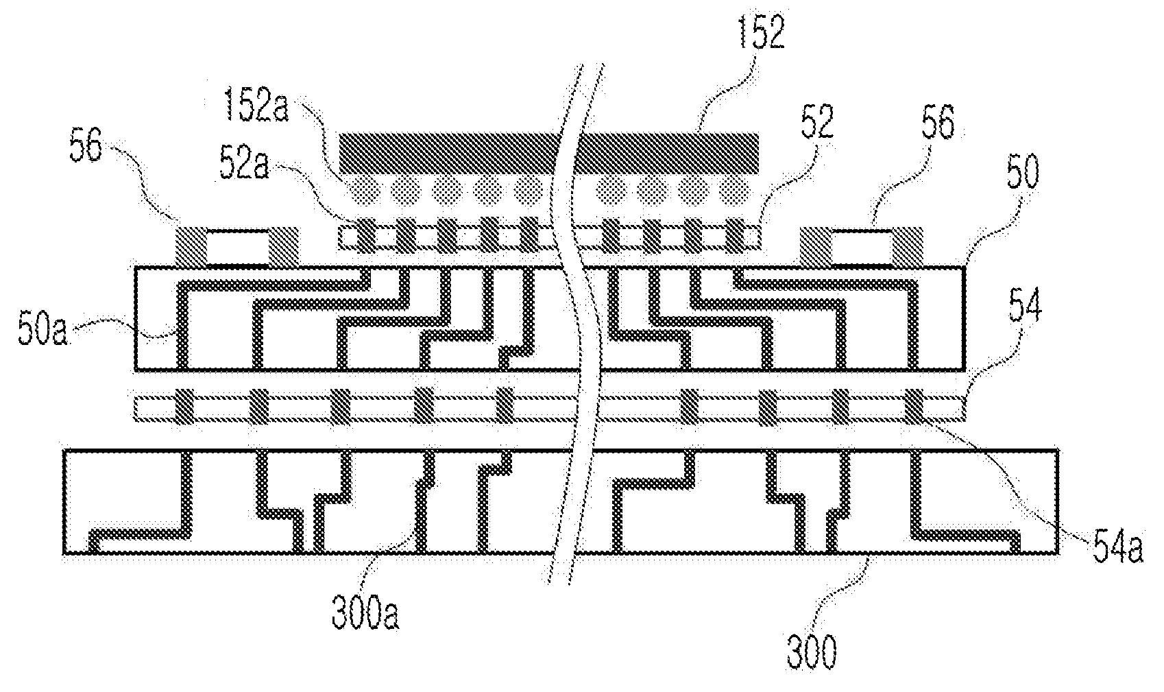
[0087]FIG. 13 is a view illustrating main configurations of a semiconductor testing apparatus according to a second exemplary embodiment of the present disclosure. FIG. 14 is an enlarged view of a middle printed circuit board, upper socket, and lower socket illustrated in FIG. 13. FIG. 15 is a view illustrating a case where a middle printed circuit board, upper socket, and lower socket illustrated in FIG. 13 are assembled. FIG. 16 is a top view of a case where a middle printed circuit board, upper socket, and lower socket are assembled. FIG. 17 is a top view of an assembled state of FIG. 13.

[0088]The test socket in the second exemplary embodiment includes a lower socket 54 mounted on an upper surface of the printed circuit board 300, a middle circuit board 50 mounted on an upper surface of the lower socket 54, and an upper socket 52 mounted on an upper surface of the middle circuit board 50. A test object (for example, semiconductor) 152 is mounted on the ...


PUM


Abstract

A semiconductor testing apparatus is provided wherein components that must be arranged most closely are arranged most closely to terminals of a test object. The present apparatus is semiconductor testing apparatus comprising a printed circuit board, and a test socket mounted on an upper surface of the printed circuit board and forming a signal connection path between a test object and the printing circuit board, wherein a chip shaped capacitor is mounted on the upper surface of the printed circuit board, an interference avoidance space avoiding contact with the capacitor is formed in the test socket, the interference avoidance space being formed at a location facing the location where the capacitor is mounted, and the capacitor and the test socket being non-contacted from each other by the interference avoidance space.

Description

BACKGROUND OF THE INVENTION[0001]1. Field[0002]The following description relates to a semiconductor testing apparatus, for example, to an apparatus for testing an object such as a semiconductor using a test socket etc.[0003]2. Description of Related Art[0004]In the case of testing an electronic device, that is an object for testing, in a conventional semiconductor signal apparatus, a testing apparatus transmits / receives signals via for example, a test head etc.[0005]FIG. 1 is a mimetic view of an overall structure of a conventional testing apparatus.[0006]A testing apparatus 100 includes a handler 150 that carries a test object device 152, a test head 130 that conducts a test on the test object device 152 carried by the handler 150, and a main frame 110 that comprehensively controls movement of the handler 150 and the test head 130. The handler 150, test head 130 and main frame 110 are connected to one another via a cable 120.[0007]The test head 130 receives a plurality of pin elect...

Claims


Application Information

Patent Timeline
IPC IPC(8): G01R31/26
CPCG01R1/0483H05K1/0231G01R1/045H05K2201/10636G01R31/2601H05K1/181H01L2224/16225H01L2924/15174H01L2924/19105Y02P70/50G01R31/26H01R33/76H05K1/18
Inventor PARK, SUNG-HAK
Owner SEMICONTEST
Why Eureka
Try Eureka