Solar cell unit and method for manufacturing the same

Inactive Publication Date: 2013-10-24
SUNOVEL SUZHOU TECH
View PDF0 Cites 8 Cited by
  • Summary
  • Abstract
  • Description
  • Claims
  • Application Information

AI Technical Summary

Benefits of technology

The present invention provides a solar cell unit with uniform doping at its side surfaces, which reduces carrier recombination and improves light absorption efficiency. The solar cell unit also has a reverse bias effect that increases the electrical current, resulting in a build-in bypass diode. Compared to traditional solar cell units, the present invention has higher efficiency and avoids shading. Additionally, the solar cell unit has a region analogous to a Zener diode that prevents reverse breakdown damage and ensures proper operation of the entire serial circuit.

Problems solved by technology

(1) photo-generated electrons and holes may be lost due to recombination at side surfaces of the solar cell unit (i.e. surfaces intersecting two primary surfaces of the solar cell units) resulting in degradation of energy conversion efficiency.
However, the side surfaces of the solar cell units usually have both n-type doped regions and p-type doped regions concurrently, which would make it unsuitable to apply the traditional process to reduce surface carrier recombination at both the n-type doped region and the p-type doped region at the same time;
(3) a plurality of solar cell units arranged in series can increase output voltage; however, in case any one of the plurality of solar cell units is shielded from solar radiation, voltage generated on other solar cell units may drop at said solar cell unit in the shade, which consequently comes into reverse bias and causes the plurality of solar cell units in series not to output electrical energy effectively, since reverse electrical current in solar cell units is usually quite small.
Besides, when the reverse bias is greater than the reverse breakdown voltage of a solar cell unit, the solar cell unit would be damaged.
However, this solution needs the use of an extra bypass diode, which consequently increases circuit complexity and manufacturing cost.

Method used

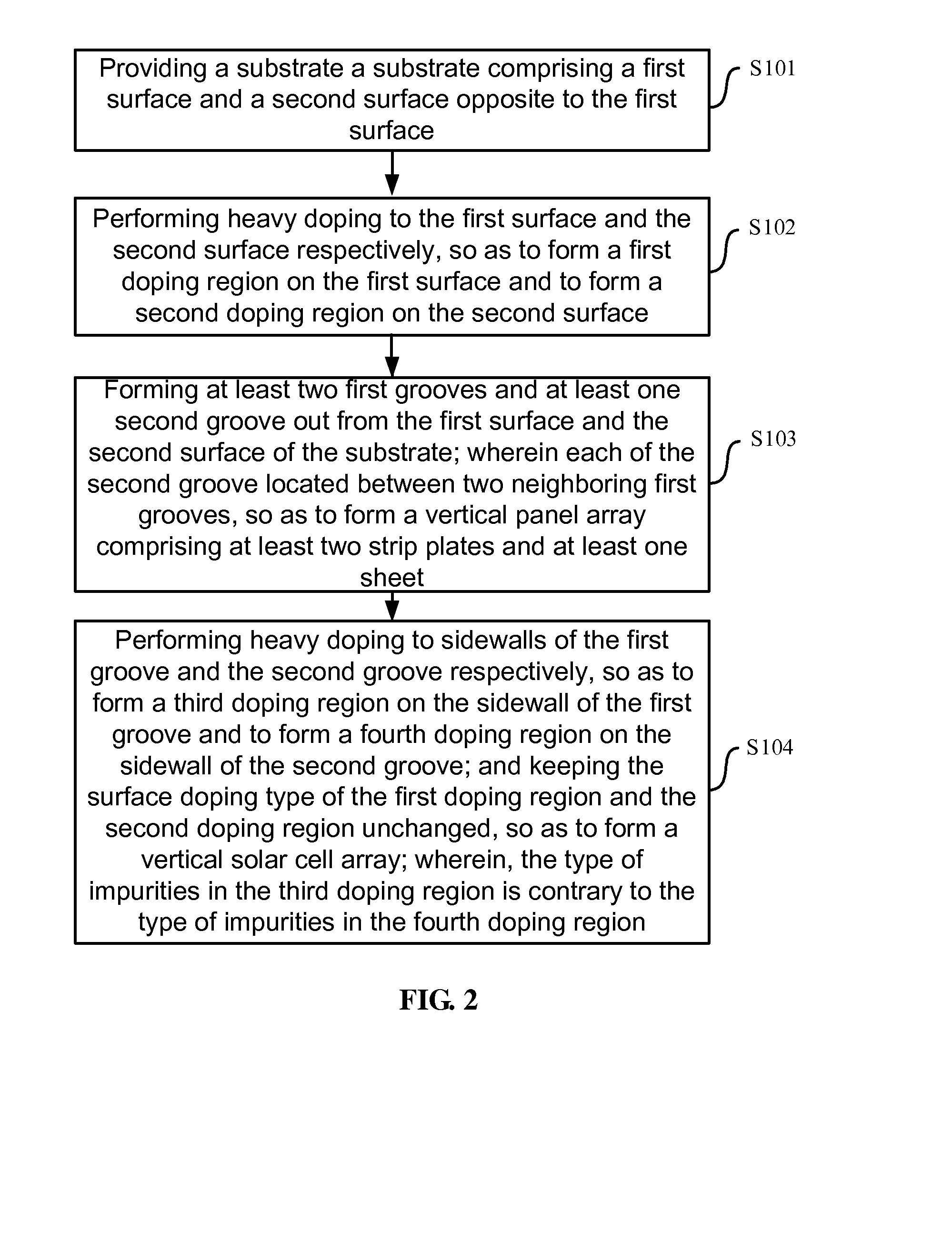

Image

  • Solar cell unit and method for manufacturing the same
  • Solar cell unit and method for manufacturing the same
  • Solar cell unit and method for manufacturing the same

Examples


Embodiment Construction

[0018]Embodiments of the present invention are to be described at length below, wherein examples of embodiments are illustrated in the appended drawings. It should be appreciated that embodiments described below in conjunction with the drawings are illustrative, and are provided for explaining the present invention only, thus shall not be interpreted as a limit to the present invention.

[0019]Various embodiments or examples are provided here below to implement different structures of the present invention. To simplify the disclosure of the present invention, descriptions of components and arrangements of specific examples are given below. They are only illustrative and not intended to limit the present invention. Moreover, in the present invention, reference numbers and / or letters may be repeated in different examples. Such repetition is for purposes of simplicity and clarity, yet does not denote any relationship between respective embodiments and / or arrangements under discussion. Fu...


PUM


Abstract

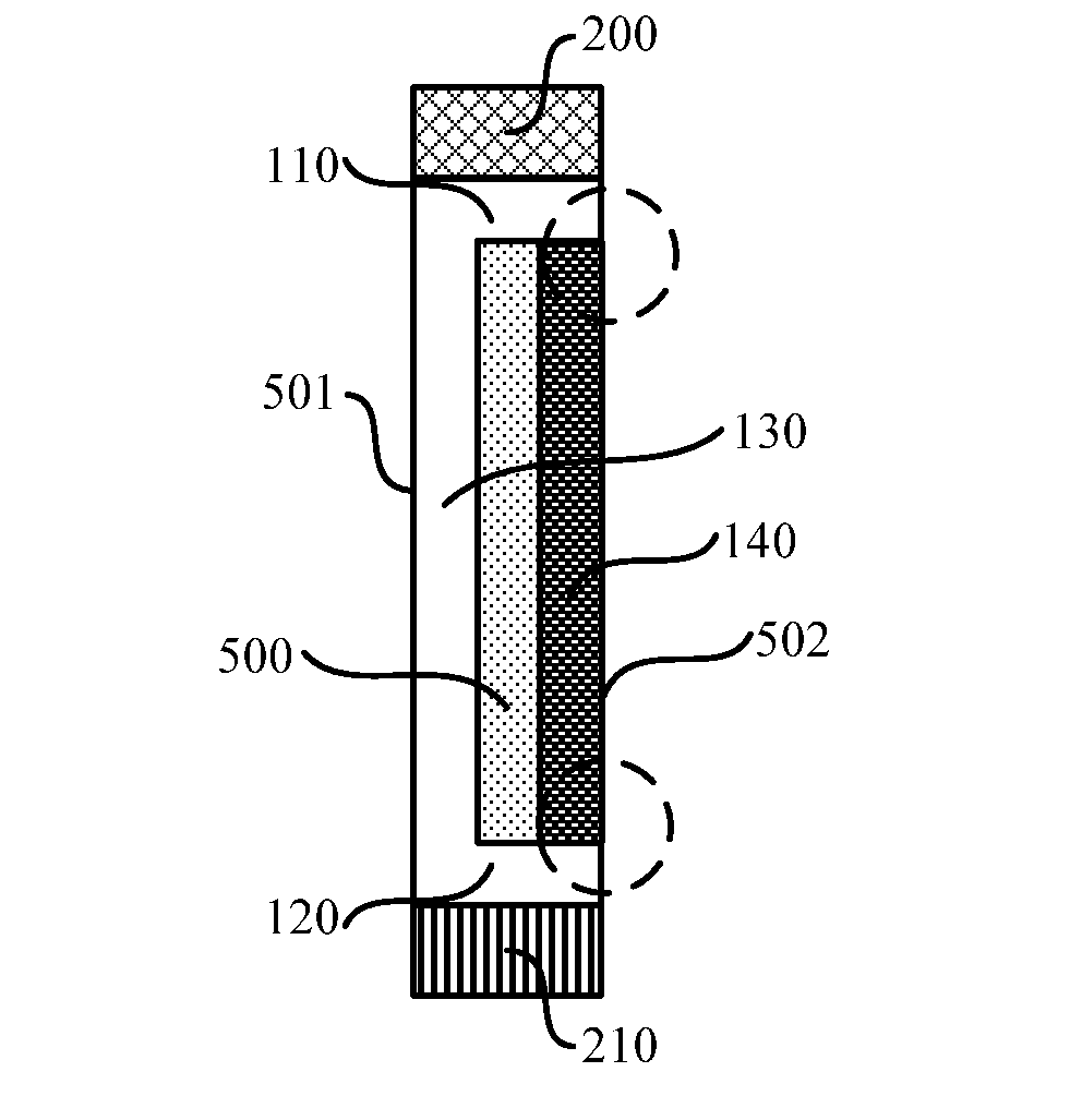
A solar cell unit comprising a strip plate which has a third surface and a fourth surface opposite to the third surface, wherein a third doping region and a fourth doping region are arranged on the third surface and the fourth surface respectively, and a first doping region and a second doping region are arranged on side surfaces adjacent to the third surface and the fourth surface respectively; the types of impurities in the third doping region and the fourth doping region are contrary to one another; the surfaces of the first doping region and the second doping region have uniform doping type. Accordingly, the present invention further provides a method for manufacturing a solar cell unit.

Description

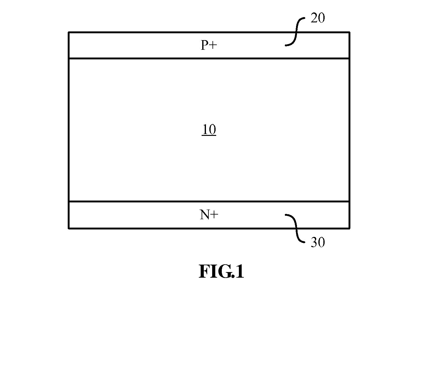
[0001]This application claims priority to Chinese Application No. 201210114584.6, filed on Apr. 19, 2012. The Chinese Application is incorporated herein by reference in its entireties.FIELD OF THE INVENTION[0002]The present invention relates to the technical field of solar cells, particularly, to a solar cell unit and a method for manufacturing the same.BACKGROUND OF THE INVENTION[0003]Due to growing concern of energy shortage and environmental challenges, solar energy has been regarded as a potential solution. At the heart of the photovoltaic industry is a solar cell which converts photon energy to electrical energy. With rapid technological advancements in the photovoltaic industry, solar cells have been widely used in various applications.[0004]As shown in FIG. 1, a solar cell unit in the prior art usually comprises a semiconductorplate 10 of p-type doped configuration or p-type doped configuration; a p+ doping region 20 is arranged on a primary surface of the semiconductor plate...

Claims


Application Information

Patent Timeline
IPC IPC(8): H01L31/0687H01L31/18
CPCH01L31/0687H01L31/1804H01L31/022425H01L31/035281H01L31/068H01L31/0443H01L31/047Y02E10/544Y02E10/547Y02P70/50
Inventor YIN, HAIZHOUZHU, HUILONGLUO, ZHIJIONG
Owner SUNOVEL SUZHOU TECH
Why Eureka
Try Eureka