Power semiconductor module

a technology of power semiconductor and semiconductor chip, applied in the direction of solid-state devices, structural fixed capacitor combinations, stacking capacitors, etc., can solve the problems of adversely affecting an external device, difficult to sufficiently suppress switching noise, and switching noise generated in the switching element, so as to reduce the size, noise, thermal resistance, cost, effect of reducing the thermal resistance between the power semiconductor chip and the insulating substra

Active Publication Date: 2013-10-24
FUJI ELECTRIC CO LTD
View PDF2 Cites 26 Cited by
  • Summary
  • Abstract
  • Description
  • Claims
  • Application Information

AI Technical Summary

Benefits of technology

[0029]According to the invention, by a capacitor being installed between the printed substrate and insulating substrate so as to be adjacent to a switching element, it is possible to reduce switching noise generated in the switching element, and furthermore, it is possible to reduce thermal resistance between the power semiconductor chip and insulating substrate. As a result of this, it is possible to provide a power semiconductor module reduced in size, noise, thermal resistance, and cost.

Problems solved by technology

The first problem is a problem of switching noise.
Switching noise with a frequency component of tens or more of kHz is generated in the switching element (IGBT or the like) by the switching operation, adversely affecting an external device.
However, as the noise filter 215 is installed outside the package of the power semiconductor module 201 so as to be distanced from the switching element (IGBT or the like) configuring the power semiconductor module 201, it is difficult to sufficiently suppress switching noise.
The second problem is a thermal problem.

Method used


Image

  • Power semiconductor module
  • Power semiconductor module
  • Power semiconductor module

Examples


working example 1

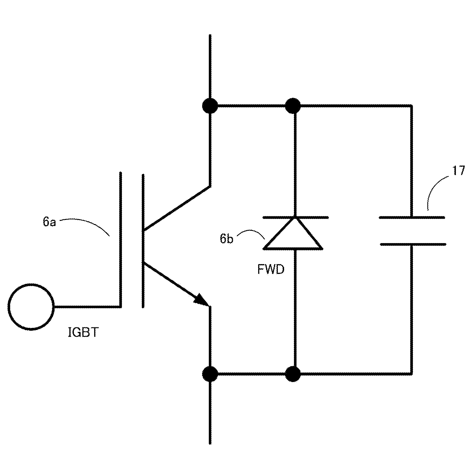
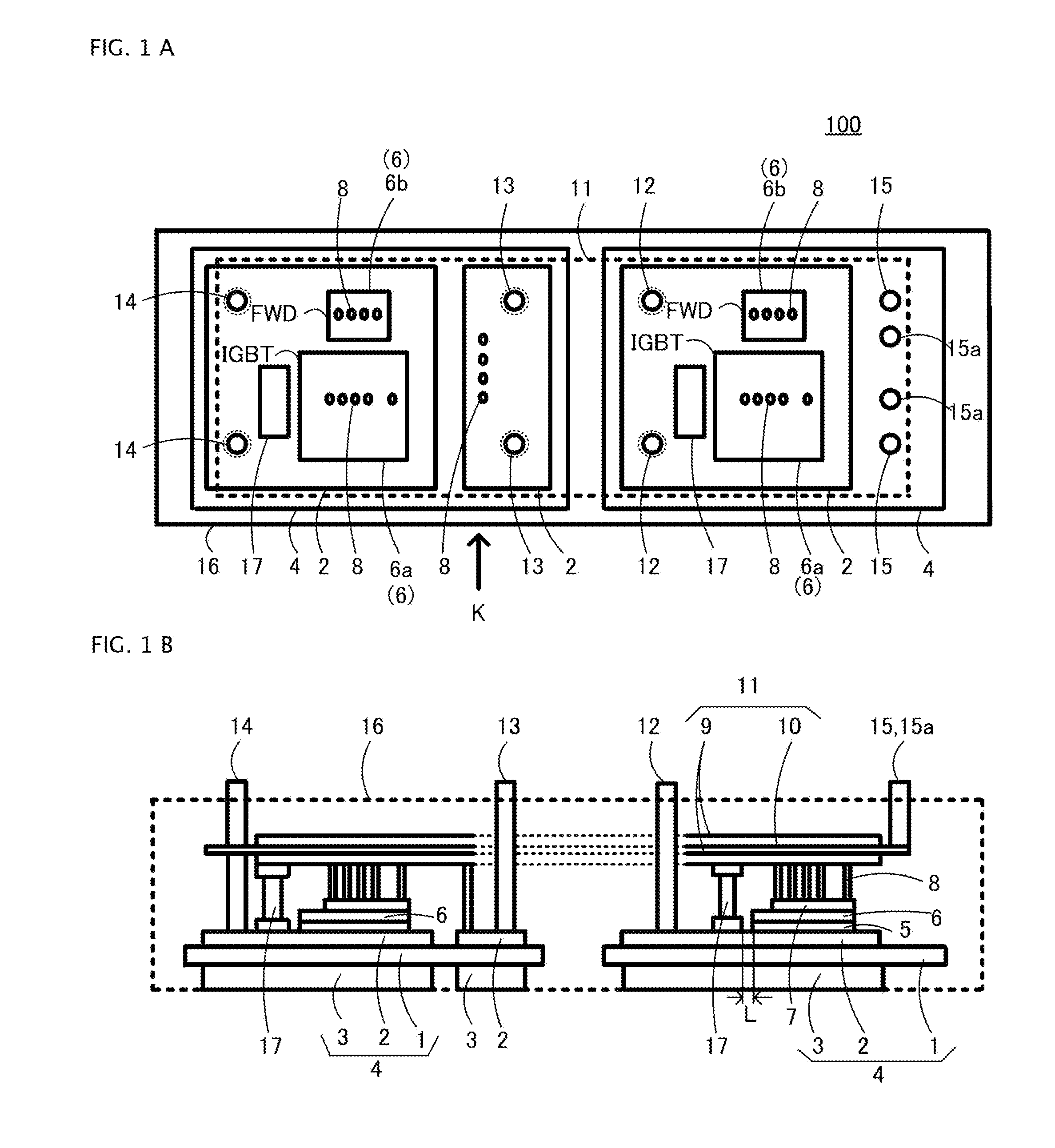
[0040]FIGS. 1A and 1B are configuration diagrams of a power semiconductor module 100 of a first working example of the invention, wherein FIG. 1A is a main portion plan view, and FIG. 1B is a main portion side view seen in the direction of an arrow K of FIG. 1A. FIG. 1A is a layout diagram of each component in a resin 16. The power semiconductor module 100 is of a type wherein main electrodes of power semiconductor chips 6 and an insulating base material 10 (printed substrate) are electrically connected by a plurality of post electrodes 8. The power semiconductor module 100, like one described as a related art, carries out a current switching, or the like, for use in a power control, or the like, using a power semiconductor.

[0041]The power semiconductor module 100 is a 2-in-1 module configured of two combinations in each of which the power semiconductor chips 6 are joined one by each solder 5 to the top of an insulating substrate 4 formed of an insulating layer 1, such as a ceramic ...

working example 2

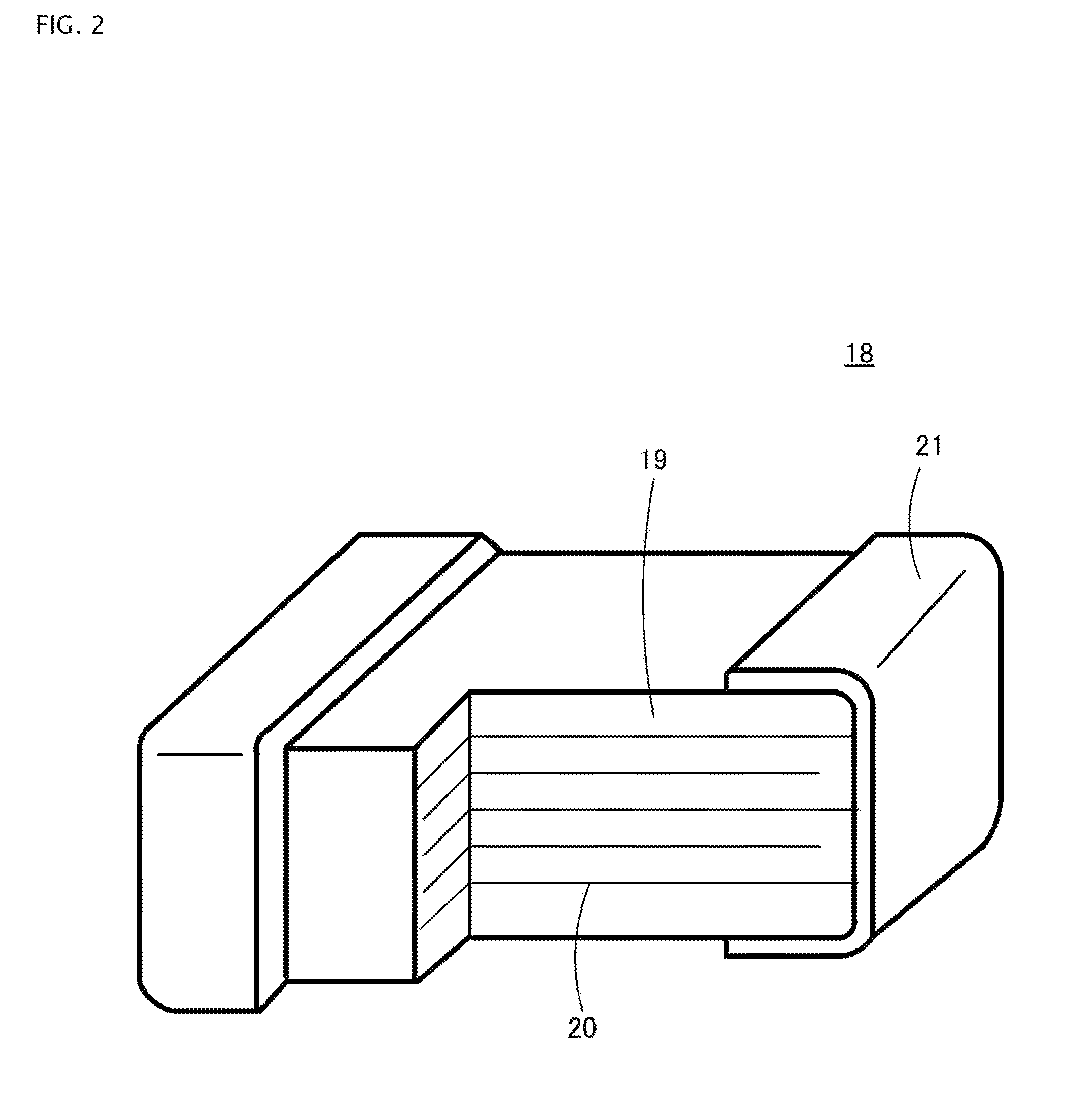
[0057]FIG. 6 is a main portion plan view of a power semiconductor module 200 of a second working example of the invention. The difference from the power semiconductor module 100 of FIGS. 1A and 1B is in that a plurality of the capacitors 17 are disposed around the power semiconductor chip 6 in each combination. By disposing the plurality of capacitors 17 in this way, the capacitance thereof becomes higher, and it is thus possible to further reduce switching noise. Furthermore, as it is possible to increase the occupation area of the capacitors 17, it is possible to further reduce the thermal resistance Rjc.

[0058]Specifically, for example, by disposing six ceramic capacitors 18 with an electrode area of 0.5 mm×0.5 mm, a height of 1 mm, and a capacitance of 50 pF around the power semiconductor chip 6, it is possible to reduce switching noise by in the order of 10% in comparison with in the case of one ceramic capacitor, and at the same time, it is possible to reduce the thermal resist...


PUM


Abstract

Embodiments of the invention provide a power semiconductor module wherein it is possible to reduce switching noise generated in a switching element, and at the same time, to reduce thermal resistance between a power semiconductor chip and an insulating substrate. In some embodiments, by a capacitor being installed between a printed substrate and an insulating substrate so as to be adjacent to a power semiconductor chip which is a switching element, it is possible to reduce switching noise generated in the switching element, and furthermore, it is possible to reduce thermal resistance between the power semiconductor chip and insulating substrate.

Description

BACKGROUND OF THE INVENTION[0001]1. Technical Field[0002]Embodiments of the invention relate to power semiconductor modules and, in particular, to power semiconductor modules wherein it is possible to reduce switching noise.[0003]2. Related Art[0004]FIGS. 7A and 7B are configuration diagrams of a heretofore known power semiconductor module 201, wherein FIG. 7A is a main portion plan view, and FIG. 7B is a main portion sectional view taken along the line A-A of FIG. 7A.[0005]The power semiconductor module 201, being a power semiconductor module of a type wherein main electrodes of power semiconductor chips 205 are electrically connected by a plurality of post electrodes 211, is described in Japanese Patent Application Publication No. JP-A-2009-64852.[0006]The power semiconductor module 201 of FIGS. 7A and 7B has an integrated structure in which an insulating substrate 202 and an implanted printed substrate 203 (hereafter the printed substrate) opposed to the insulating substrate 202 ...

Claims


Application Information

Patent Timeline
Patent Type & Authority Applications(United States)
IPC IPC(8): H01L49/02
CPCH01L28/40H01G4/30H01G4/40H01G2/065H01L2924/13055H01L2924/1305H01L2924/15787H01L24/19H01L24/29H01L24/32H01L24/73H01L25/072H01L25/16H01L2224/291H01L2224/32225H01L2224/73267H01L2924/19041H01L2924/19105H01L2924/00H01L2924/014
Inventor HORI, MOTOHITOIKEDA, YOSHINARIYAMADA, TAKAFUMI
Owner FUJI ELECTRIC CO LTD
Why Eureka
Try Eureka