Electrical interconnection structure and electrical interconnection method

a technology of electrical interconnection and three-dimensional chipset, applied in the direction of semiconductor devices, semiconductor/solid-state device details, electrical apparatus, etc., can solve the problems of signal transmission error, reduced signal integrity, and waveform of electrical signals, so as to improve operation speed and bandwidth, improve the effect of impedance matching performance and adjusting capacitan

Inactive Publication Date: 2013-10-24
SILICONWARE PRECISION IND CO LTD
View PDF2 Cites 4 Cited by
  • Summary
  • Abstract
  • Description
  • Claims
  • Application Information

AI Technical Summary

Benefits of technology

[0014]The present invention further provides an electrical interconnection method for reducing impedance mismatch in a three-dimensional (3D) chipset, which comprises the steps of: forming a first signal circuit and a first grounding layer on a first surface of a substrate such that the first grounding layer surrounds the first signal circuit along the pathway of the first signal circuit; forming a first TSV and a second TSV in the substrate such that one end of the first TSV is connected to the first signal circuit and one end of the second TSV is connected to the first grounding layer, the end of the first TSV being surrounded by the first grounding layer with a gap formed therebetween; forming a second signal circuit and a second grounding layer on a second surface of the substrate opposite to the first surface such that the second grounding layer surrounds the second signal circuit along the pathway of the second signal circuit, wherein the other end of the first TSV is surrounded by the second grounding layer with a gap formed therebetween; and changing the gaps so as to adjust the capacitance between the grounding layers and the signal circuits, thereby regulating the impedance between the signal circuits and the grounding layers.
[0017]Compared with the prior art, the present invention can adjust the capacitance between the grounding layers and the signal circuits by changing the gaps between the grounding layers and the ends of the first TSV, thereby regulating the impedance therebetween. Therefore, the present invention can achieve a preferred impedance match performance so as to increase the operation speed and bandwidth in the 3D chip stacking technologies.

Problems solved by technology

Therefore, an obvious impedance mismatch (or discontinuity) can occur between the signal transmission structure 11 and the grounding structures 12a and 12b. For example, a high impedance variation k (usually 20% variation) is shown in FIG. 1B, which severely affects the waveform of the electrical signal and even reduces the signal integrity so as to result in a signal transmission error.
As such, it is difficult to increase the operation speed and bandwidth of the structure due to a poor impedance match.

Method used


Image

  • Electrical interconnection structure and electrical interconnection method
  • Electrical interconnection structure and electrical interconnection method
  • Electrical interconnection structure and electrical interconnection method

Examples


Embodiment Construction

[0022]The following illustrative embodiments are provided to illustrate the disclosure of the present invention, these and other advantages and effects can be apparent to those in the art after reading this specification.

[0023]It should be noted that the drawings are only for illustrative purposes and not intended to limit the present invention. Meanwhile, terms such as ‘end’, ‘on’, ‘a’ etc. are only used as a matter of descriptive convenience and not intended to have any other significance or provide limitations for the present invention.

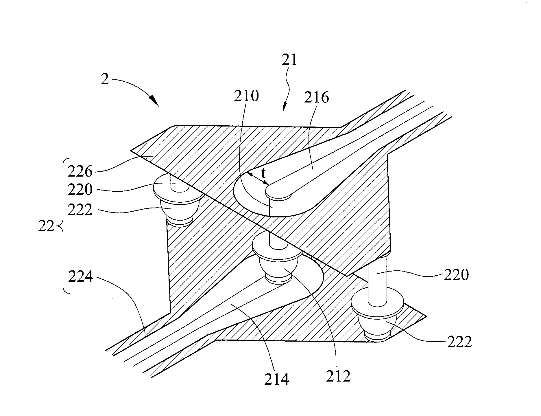
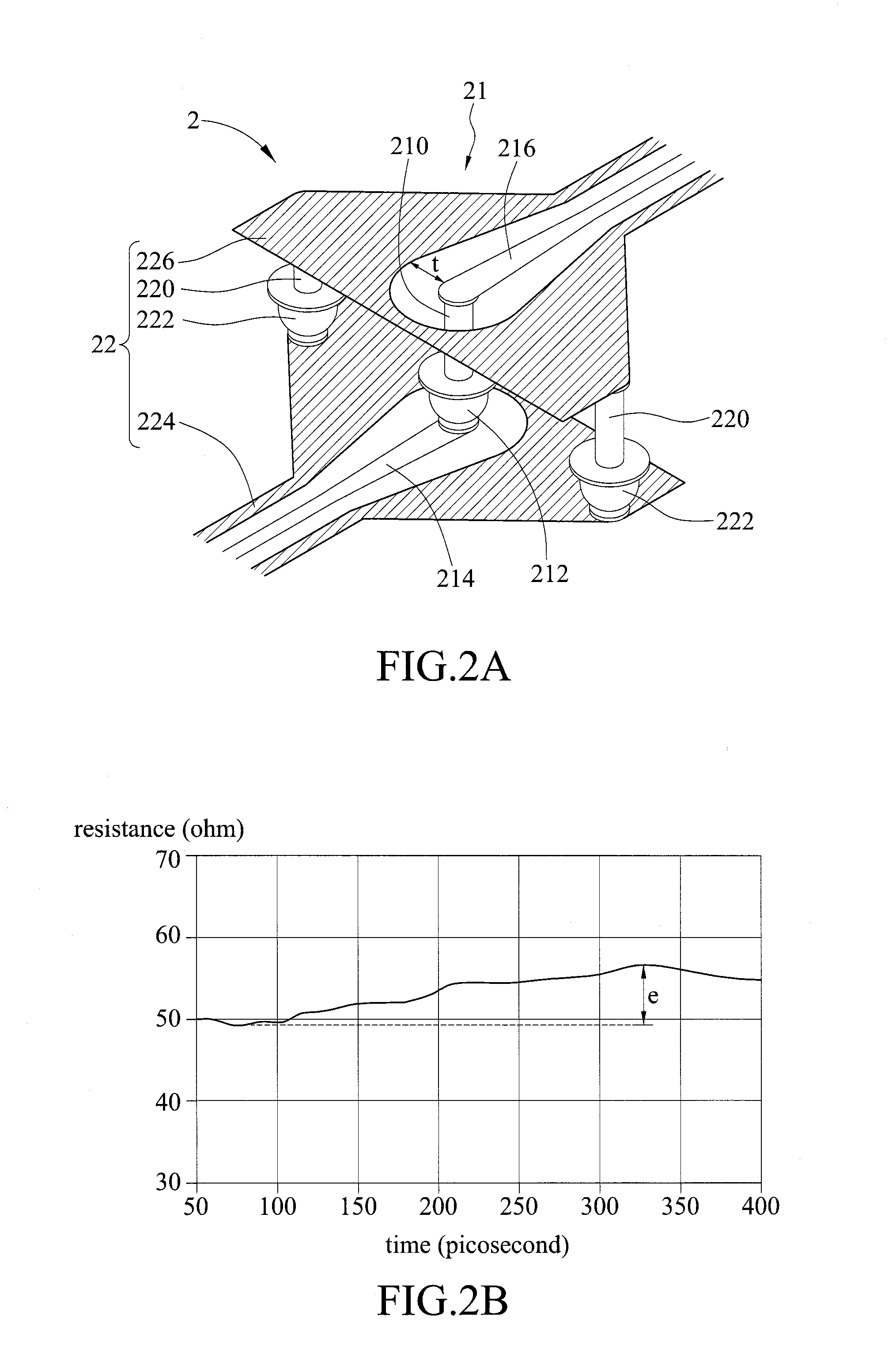
[0024]FIG. 2A is a schematic perspective view showing an electrical interconnection structure 2 according to the present invention. Referring to FIG. 2A, the electrical interconnection structure 2 has a signal transmission structure 21 and a grounding structure 22.

[0025]The signal transmission structure 21 has a first TSV 210, a lower signal circuit 214, an upper signal circuit 216 and a conductive bump 212. The grounding structure 22 has two secon...


PUM


Abstract

An electrical interconnection structure includes: a signal transmission structure having a first through silicon via (TSV) and signal circuits connected to two opposite ends of the first TSV, respectively; and a grounding structure having a second TSV and grounding layers connected to two opposite ends of the second TSV, respectively. The grounding layers surround the signal circuits along the pathways thereof such that the ends of the first TSV are surrounded by the grounding layers with gaps therebetween. By changing the gaps between the grounding layers and the ends of the first TSV, the capacitance between the grounding layers and the signal circuits is adjusted so as to regulate the impedance therebetween.

Description

BACKGROUND OF THE INVENTION[0001]1. Field of the Invention[0002]The present invention relates to semiconductor stacking technologies, and, more particularly, to an electrical interconnection structure and electrical interconnection method in a three-dimensional (3D) chipset.[0003]2. Description of Related Art[0004]Along with the increasing demands of consumers for multi-functional and miniaturized electronic products, more and more electronic components and functions have to be integrated in a given area of a substrate. Accordingly, three-dimensional stacking technologies are developed.[0005]Furthermore, redistribution layers (RDL), through silicon vias (TSV) and conductive bumps are provided to serve as electrical interconnection structures for signal transmission so as to increase the operation speed and bandwidth.[0006]FIG. 1A is a schematic perspective view of a conventional electrical interconnection structure 1. Referring to FIG. 1A, the electrical interconnection structure 1 ...

Claims


Application Information

Patent Timeline
Patent Type & Authority Applications(United States)
IPC IPC(8): H01L23/48
CPCH01L23/481H01L23/5225H01L25/0657H01L2224/0401H01L2224/0557H01L2224/16146H01L2224/16227H01L2225/06527H01L23/64H01L2225/06513H01L2225/06544H01L2224/16225H01L21/76898H01L2924/00014H01L2224/05552
Inventor SUNG, TSE-SHIHCHIANG, WEN-JUNGLEE, HSIN-HUNG
Owner SILICONWARE PRECISION IND CO LTD
Why Eureka
Try Eureka