Semiconductor device

a technology of semiconductors and semiconductors, applied in the direction of power consumption reduction, pulse techniques, instruments, etc., can solve the problems of difficult to reduce the power consumption of memory elements, delay in processing, and inability to retain data, so as to increase the execution speed of applications. , the effect of low power consumption

Inactive Publication Date: 2013-10-31
SEMICON ENERGY LAB CO LTD
View PDF3 Cites 12 Cited by
  • Summary
  • Abstract
  • Description
  • Claims
  • Application Information

AI Technical Summary

Benefits of technology

[0018]One embodiment of the present invention can provide a semiconductor device including a PLD which can increase the execution speed of an application. One emb...

Problems solved by technology

In addition, in the case where configuration data is transferred by a DMAC, transmission of other data needed for operation of the processor is interrupted, so that the operation of the processor is delayed.
However, an SRAM not only consumes power in an operating state but also consumes more than a little power in a non-operating state because of an off-state current of a transistor, and an DRAM consumes power by a refresh operation; thus, it is difficult for th...

Method used


Image

  • Semiconductor device
  • Semiconductor device
  • Semiconductor device

Examples


embodiment 1

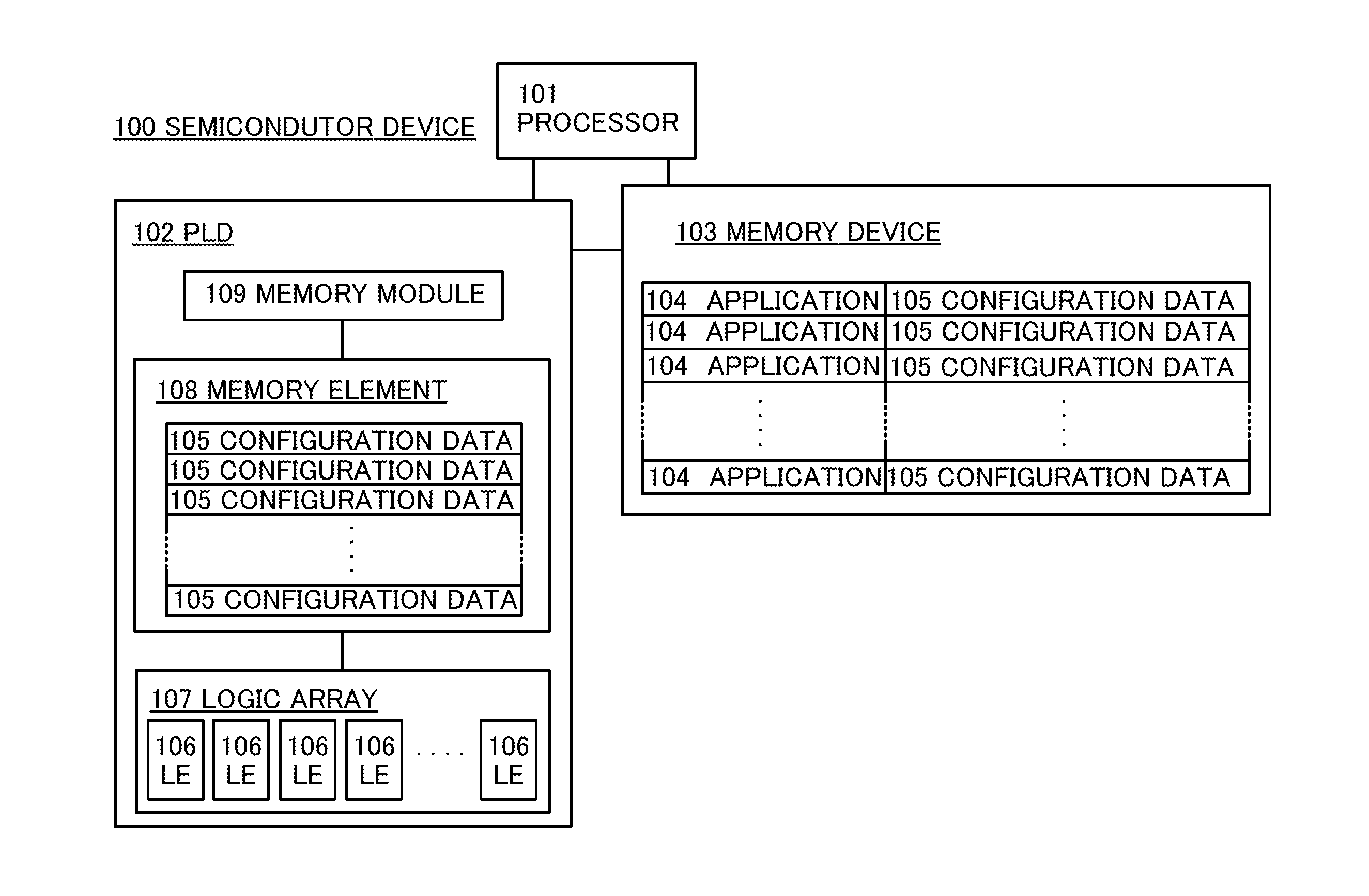
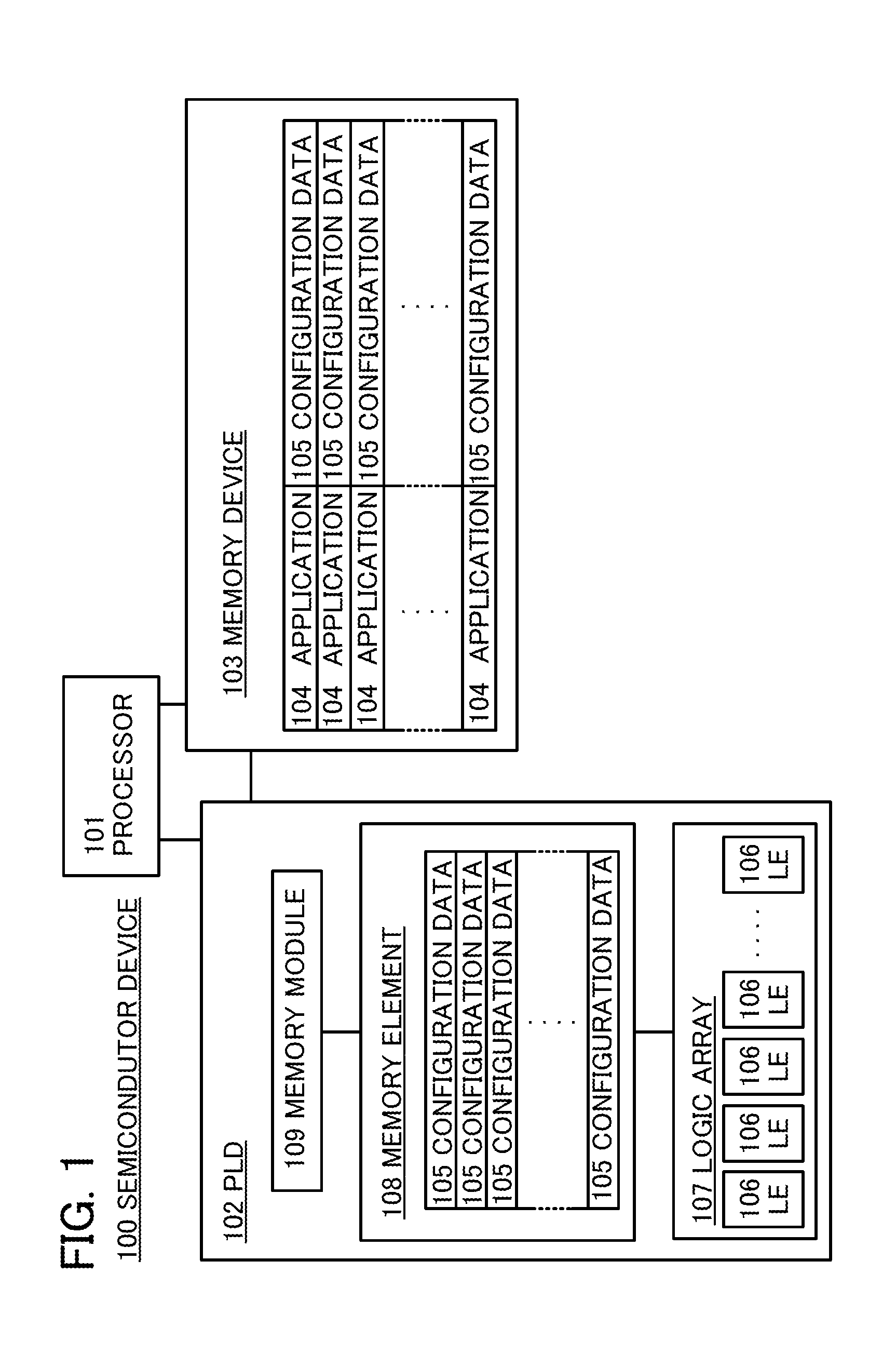
[0035]FIG. 1 is a block diagram illustrating a configuration example of a semiconductor device 100 of one embodiment of the present invention. Note that in a block diagram in this specification, circuits are classified in accordance with their functions and illustrated as independent blocks. However, it is difficult to classify actual circuits according to their functions completely and it is possible for one circuit to have a plurality of functions.

[0036]The semiconductor device 100 illustrated in FIG. 1 includes a processor 101, a PLD 102, and a storage device 103. The circuit configuration of the processor 101 is fixed and is not dynamically reconfigured. The circuit configuration of the PLD 102 is not fixed and can be dynamically reconfigured.

[0037]The storage device 103 is nonvolatile and a plurality of applications 104 executed by the processor 101 and a plurality of pieces of configuration data 105 related to respective applications 104 are stored in the storage device 103. A...

embodiment 2

[0177]The semiconductor device of one embodiment of the present invention can be used for display devices, personal computers, and image reproducing devices provided with recording media (typically, devices that reproduce the content of recording media such as digital versatile discs (DVDs) and have displays for displaying the reproduced images). Other examples of electronic devices that can include the semiconductor device of one embodiment of the present invention are mobile phones, game machines including portable game consoles, portable information terminals, e-book readers, video cameras, digital still cameras, goggle-type displays (head mounted displays), navigation systems, audio reproducing devices (e.g., car audio systems and digital audio players), copiers, facsimiles, printers, multifunction printers, automated teller machines (ATM), and vending machines. FIGS. 14A to 14D illustrate specific examples of these electronic devices.

[0178]FIG. 14A illustrates a portable game c...


PUM


Abstract

A semiconductor device including a PLD which can increase the execution speed of an application with low power consumption is provided. The semiconductor device includes a programmable logic device and a processor which is not dynamically reconfigured. A memory element of the programmable logic device stores a plurality of pieces of configuration data determined to have high frequency of use by a memory module among configuration data corresponding to a thread. The memory element includes a storage element and a switch in each of a plurality of memory cells. The switch is used for supplying charge whose amount is determined by the plurality of pieces of stored configuration data to the storage element, retaining the charge in the storage element, and discharging the charge from the storage element.

Description

BACKGROUND OF THE INVENTION[0001]1. Field of the Invention[0002]The present invention relates to a semiconductor device including a programmable logic device which can change a configuration of hardware.[0003]2. Description of the Related Art[0004]Smaller and lighter mobile information terminals such as PDAs and smartphones are highly required by users; thus, the scale of hardware that can be built in the limited space in a housing is limited. However, the mobile information terminals are required to have a number of functions, for example, functions of playing moving images, supporting online games, recognizing voice, and capturing images using a miniature camera, so that a plurality of application programs (hereinafter, referred to as applications) needs to be executed using the hardware. The larger the number of applications to be executed is and the smaller the scale of the hardware is, the smaller the storage area which can be secured in a buffer storage device is. This causes ...

Claims


Application Information

Patent Timeline
IPC IPC(8): H03K19/00
CPCH03K19/0008H03K19/17756H03K19/17784
Inventor FUKUTOME, TAKAHIRO
Owner SEMICON ENERGY LAB CO LTD
Why Eureka
Try Eureka