Member for semiconductor manufacturing apparatus

a manufacturing apparatus and semiconductor technology, applied in the direction of electrostatic holding devices, electric devices, basic electric elements, etc., can solve the problems of unfavorable thermal uniformity shift, difficult uniform processing of wafers, and sometimes shifts in thermal uniformity, so as to achieve favorable thermal uniformity in the initial state, easy construction, and favorable thermal uniformity

Active Publication Date: 2013-10-31
NGK INSULATORS LTD
View PDF4 Cites 41 Cited by
  • Summary
  • Abstract
  • Description
  • Claims
  • Application Information

AI Technical Summary

Benefits of technology

[0011]In the member for a semiconductor manufacturing apparatus of the present invention, the spring members are preferably coil springs. In this case, compared to a case where the spring members are spring washers, the thermal uniformity in the initial state is favorable. In the case of spring washers, the pressure that presses the electrostatic chuck and the cooling unit does not easily become constant even if tightening is performed with a predetermined tightening torque. In contrast, in the case of coil springs, such pressure easily becomes constant, and the thermal uniformity in the initial state is favorable.
[0012]In the member for a semiconductor manufacturing apparatus of the present invention, the screw feet of the screws may pass through the clamp ring and the cooling unit from the clamp ring side, and after the screw feet pass through the cooling unit, nuts may be screwed on the screw feet, with the spring members therebetween. In this case, a structure in which the spring members are placed on the cooling unit side can be easily constructed.
[0013]In the member for a semiconductor manufacturing apparatus of the present invention, heat-transfer gas may be supplied to the gap. In this case, heat exchange between the electrostatic chuck and the cooling unit is performed through the heat-transfer gas, and therefore the thermal uniformity improves further.
[0014]In the member for a semiconductor manufacturing apparatus of the present invention, a dot-like outer periphery spacer may be placed at a position where a gap outer peripheral part of the gap along the outer periphery of the electrostatic chuck intersects with a radial direction from the center of the electrostatic chuck toward the screw. In this case, when the clamp ring is fastened with screws, the electrostatic chuck is not pressed like a cantilever, and therefore the electrostatic chuck can be prevented from being damaged. In this case, the dot-like outer periphery spacer is preferably integrated with a spacer support that is formed in a ring-like shape so as to protrude outwardly from the gap. When the outer periphery spacer is dot-like, the outer periphery spacer is sometimes displaced. However, here the dot-like outer periphery spacer is integrated with the ring-like spacer support, and is therefore not displaced. In addition, since the spacer support is protruding outwardly from the gap, the spacer support hardly promotes the heat transfer between the electrostatic chuck and the cooling unit. Therefore, the outer periphery spacer hardly affects the thermal uniformity.
[0015]In the member for a semiconductor manufacturing apparatus of the present invention, a ring-like outer periphery spacer may be placed in a gap outer peripheral part of the gap along the outer periphery of the electrostatic chuck. Also in this case, when the clamp ring is fastened with screws, the electrostatic chuck is not pressed like a cantilever, and therefore the electrostatic chuck can be prevented from being damaged. When the outer periphery spacer is dot-like, the outer periphery spacer is sometimes displaced. However, here the outer periphery spacer is ring-like, and is therefore not displaced.
[0016]In the member for a semiconductor manufacturing apparatus of the present invention, when it has the outer periphery spacer, the outer periphery spacer is preferably made of polyimide resin. The outer periphery spacer may be made of fluororesin such as polytetrafluoroethylene. Since polyimide resin is harder, the outer periphery spacer is less deformable, and the screws are less likely to come loose. As a result, the thermal uniformity is less likely to shift.

Problems solved by technology

However, in this member for a semiconductor manufacturing apparatus, the thermal uniformity sometimes shifts with repeated use.
A shift in the thermal uniformity is unfavorable because it makes it difficult to uniformly process a wafer.

Method used


Image

  • Member for semiconductor manufacturing apparatus
  • Member for semiconductor manufacturing apparatus
  • Member for semiconductor manufacturing apparatus

Examples


example 2

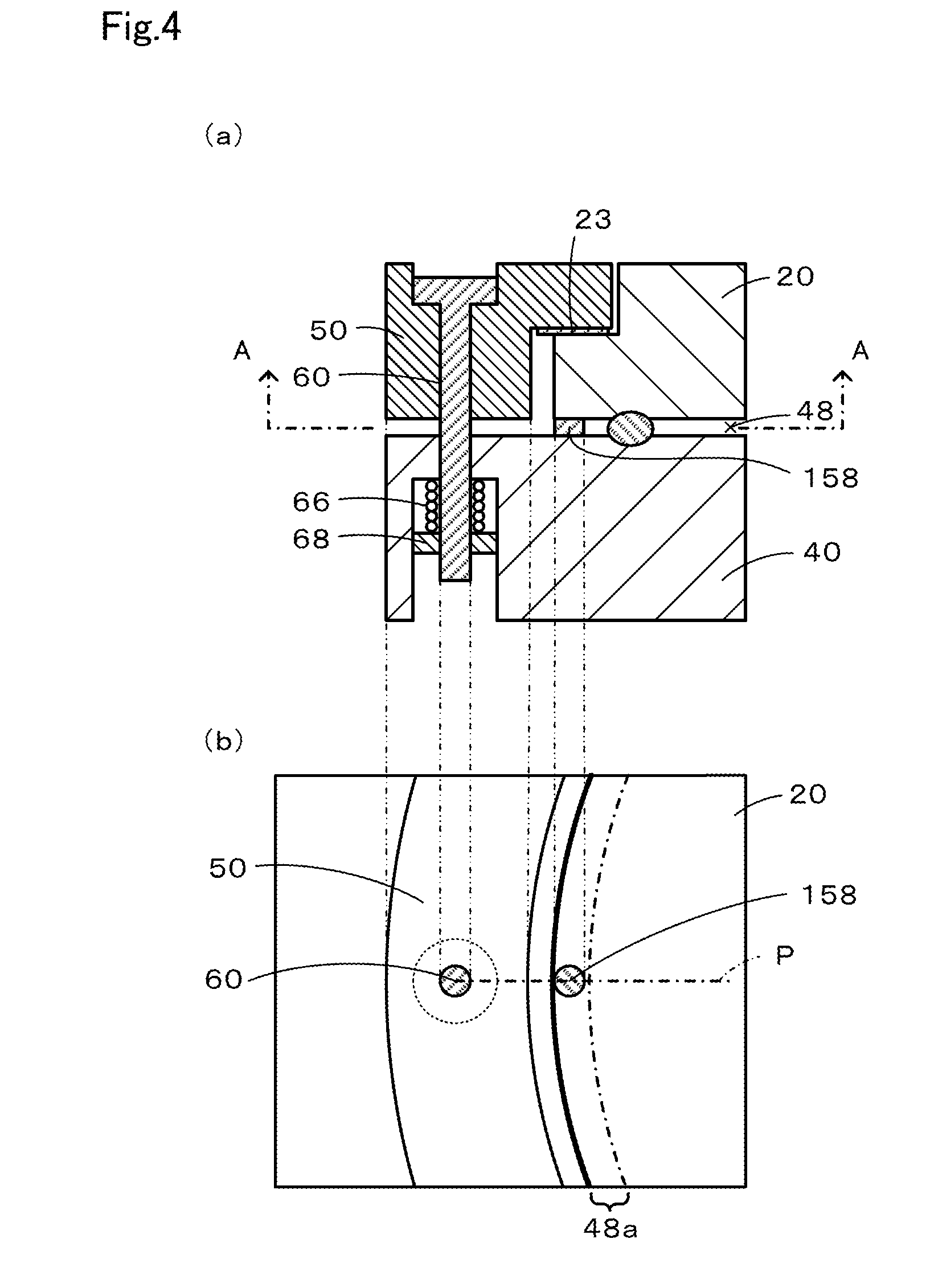
[0038]FIG. 4 is an explanatory diagram of Example 2, (a) is an enlarged longitudinal sectional view of the clamp ring and its vicinity, and (b) is a sectional view taken along line A-A of (a). In FIG. 4 (b), the outer peripheral edge of the electrostatic chuck 20 is shown by a heavy line. In Example 2, instead of the outer periphery spacer 58 of Example 1, a dot-like outer periphery spacer 158 made of polytetrafluoroethylene was used. This outer periphery spacer 158 is placed in a gap outer peripheral part 48a of the gap 48 along the outer periphery of the electrostatic chuck 20. Specifically, the outer periphery spacer 158 is placed at a position where the gap outer peripheral part 48a intersects with a radial direction P from the center of the electrostatic chuck 20 toward the screw 60. In Example 2, when the clamp ring 50 was fastened using screws 60, coil springs 66, and nuts 68, the electrostatic chuck 20 was not damaged in the stepped portion 23. Although the outer periphery s...

example 3

[0039]A member for a semiconductor manufacturing apparatus that was the same as Example 2 (FIG. 4) except that the material of the outer periphery spacer 158 was changed to polyimide was made. In Example 3, when the clamp ring 50 was fastened using screws 60, coil springs 66, and nuts 68, the electrostatic chuck 20 was not damaged in the stepped portion 23. In addition, since the outer periphery spacer 158 was dot-like, no cool spot was generated in the outer peripheral part of the electrostatic chuck 20. Further, since the material of the outer periphery spacer 158 was hard, the outer periphery spacer 158 was not deformed over time, and the thermal uniformity did not shift owing to the loose of the screws 60. However, since the material of the outer periphery spacer 158 was hard and the outer periphery spacer 158 was less deformable when screws were tightened, the outer periphery spacer 158 was sometimes displaced.

example 4

[0040]FIG. 5 is an explanatory diagram of Example 4, (a) is an enlarged longitudinal sectional view of the clamp ring and its vicinity, and (b) is a sectional view taken along line B-B of (a). In FIG. 5 (b), the outer peripheral edge of the electrostatic chuck 20 is shown by a heavy line. In Example 4, instead of the outer periphery spacer 58 of Example 1, a ring-like outer periphery spacer 258 made of polyimide was used. This outer periphery spacer 258 is placed in a gap outer peripheral part 48a of the gap 48 along the outer periphery of the electrostatic chuck 20. In Example 4, when the clamp ring 50 was fastened using screws 60, coil springs 66, and nuts 68, the electrostatic chuck 20 was not damaged in the stepped portion 23. In addition, since the material of the outer periphery spacer 258 was hard, the outer periphery spacer 258 was not deformed over time, and the thermal uniformity did not shift owing to the loose of the screws 60. Further, since the outer periphery spacer 2...


PUM


Abstract

A member 10 for a semiconductor manufacturing apparatus includes an electrostatic chuck 20, a cooling unit 40, a spacer (an O-ring 44, an outer periphery spacer 58, or the like) for securing a gap 48 placed between the electrostatic chuck 20 and the cooling unit 40, and a clamp ring 50 placed on the upper surface of the outer periphery of the electrostatic chuck 20. The clamp ring 50 is fastened to the cooling unit 40 with screws 60. The screws 60 are inserted into coil springs 66 that prevent loosening, and are fastened to nuts 68. The coil springs 66 are attached not to the clamp ring side but to the cooling unit side.

Description

BACKGROUND OF THE INVENTION[0001]1. Field of the Invention[0002]The present invention relates to a member for a semiconductor manufacturing apparatus.[0003]2. Description of the Related Art[0004]Hitherto, there has been known a member for a semiconductor manufacturing apparatus in which an electrostatic chuck having a wafer placing surface is provided on a cooling unit. Such a member for a semiconductor manufacturing apparatus in which for the purpose of taking heat from a wafer placed on the electrostatic chuck, back side gas such as helium (He) is caused to flow to the back side of the wafer has been known (see, for example, PTL 1).CITATION LISTPatent Literature[0005][PTL 1] Japanese Unexamined Patent Application Publication No. 2000-315680SUMMARY OF THE INVENTION[0006]It is conceivable that in such a member for a semiconductor manufacturing apparatus, a spacer for securing a gap is placed between the electrostatic chuck and the cooling unit, and the electrostatic chuck and the co...

Claims


Application Information

Patent Timeline
Patent Type & Authority Applications(United States)
IPC IPC(8): H02N13/00
CPCH02N13/00H01L21/67109H01L21/6831H01L21/68721H01L21/68785
Inventor TAKASAKI, HIDEAKIKATAIGI, TAKASHI
Owner NGK INSULATORS LTD
Why Eureka
Try Eureka