IGBT device capable of improving switch-on and switch-off speed and switch-on and switch-off uniformity and manufacturing method thereof

A technology of switching speed and uniformity, applied in the field of power devices and their manufacturing, can solve the problems of poor switching uniformity, slow switching speed of IGBT devices, and speed up the transmission speed of gate voltage, so as to reduce switching loss, realize simple structure, and improve Effects of switching speed and switching uniformity

Active Publication Date: 2014-02-12
STATE GRID CORP OF CHINA +2
View PDF5 Cites 9 Cited by
  • Summary
  • Abstract
  • Description
  • Claims
  • Application Information

AI Technical Summary

Problems solved by technology

[0009] For the deficiencies in the prior art, the purpose of the present invention is to provide a kind of IGBT device that enhances switching speed and switching uniformity, and another purpose is to provide the manufacturing method of the IGBT device that strengthens switching speed and switching uniformity, the present invention passes Gate Finger The aluminum lead directly transmits the gate voltage on the gate PAD to the aluminum lead in the gate Bus area, which speeds up the transmission speed of the gate voltage, and simultaneously transmits the voltage to the cells in each emitter PAD area 01 from four sides, reducing the The turn-on or turn-off time of the IGBT reduces the turn-on or turn-off loss, improves the uniformity of the IGBT switch, and solves the problem of slow switching speed and poor switch uniformity of the IGBT device

Method used


Image

  • IGBT device capable of improving switch-on and switch-off speed and switch-on and switch-off uniformity and manufacturing method thereof
  • IGBT device capable of improving switch-on and switch-off speed and switch-on and switch-off uniformity and manufacturing method thereof
  • IGBT device capable of improving switch-on and switch-off speed and switch-on and switch-off uniformity and manufacturing method thereof

Examples


Embodiment 1

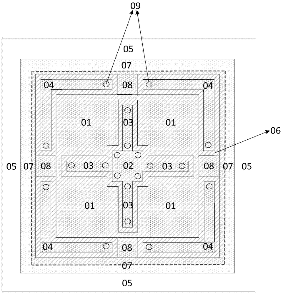
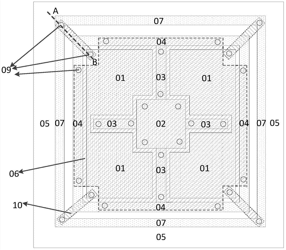
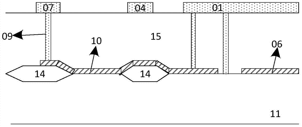
[0052] Embodiment 1 (with figure 2 Take the generation process of the cross-sectional diagram of the dotted line AB as an example)

[0053] The present invention also provides a method for manufacturing an IGBT device with enhanced switching speed and switching uniformity, comprising the following steps:

[0054] (1) A thin oxide layer is grown on the uniformly doped N-type substrate 11 as a barrier layer, and after processes such as coating, exposure, development, and deglue, the field-limiting ring P-Ring12 doped in the terminal area is engraved The window is P-Ring doped by ion implantation. After the same process, the N-Ring13 doping of the field limiting ring in the terminal area is carried out, such as Figure 4 shown.

[0055] (2) Field oxide layer 14: use high temperature oxidation method to grow a thick oxide layer on the surface of the silicon wafer, use the field oxide layer photolithography plate, go through glue coating, exposure, development, oxide film etchi...


PUM


Abstract

The invention relates to a power device and a manufacturing method of the power device, in particular to an IGBT device capable of improving the switch-on and switch-off speed and switch-on and switch-off uniformity and a manufacturing method of the IGBT device. The IGBT device comprises emitting electrode PAD regions, a grid PAD region, grid Finger regions, a grid Bus region and a terminal region. The grid PAD region is located at the center of the device, the emitting electrode PAD regions are distributed around the grid PAD region and separated by the grid Finger regions, the grid Bus region surrounds the emitting electrode PAD regions, and the terminal region is located on the periphery of the grid Bus region. By improving the traditional structural design of a polycrystalline silicon layer and a metal layer, the speed of charging and discharging cellular grids is improved when the IGBT device is switched on or switched off, and accordingly the overall switch-on and switch-off speed of the IGBT device is improved. Compared with a traditional IGBT device structure, the IGBT device has the advantages that the switch-on and switch-off speed of the IGBT device is improved, and the switch-on and switch-off uniformity of IGBT cells is improved at the same time.

Description

technical field [0001] The invention relates to a power device and a manufacturing method thereof, in particular to an IGBT device with enhanced switching speed and switching uniformity and a manufacturing method thereof. Background technique [0002] PAD area: The window opened on the passivation layer of the chip. When packaging, wires are welded on it, connected to the pins, and the potential is drawn out. Specifically, there are gate PAD area and emitter PAD area. [0003] Gate Bus area: In order to ensure that the edge cells are turned on or off at the same time, the edge cells are usually surrounded by a metal ring, and then the gate potential is transmitted through polysilicon. [0004] Gate Finger area: In order to reduce the influence of the distributed resistance of the gate electrode material, polysilicon and metal are usually used to lead the gate potential to the cell unit far away from the gate PAD. [0005] IGBT (Insulated Gate Bipolar Transistor), that is, ...

Claims


Application Information

Patent Timeline
Patent Type & Authority Applications(China)
IPC IPC(8): H01L29/739H01L23/49H01L23/498H01L29/06H01L21/331H01L21/48
CPCH01L24/05H01L2224/05552H01L2924/1305H01L2924/13055H01L2924/13091H01L2924/00
Inventor 何敏高文玉刘江吴迪王耀华刘隽凌平包海龙张宇
Owner STATE GRID CORP OF CHINA
Why Eureka
Try Eureka