

Etch remnant removal
a remnant and etching technology, applied in the direction of cleaning process and apparatus, electric discharge tube, chemical apparatus and processes, etc., can solve the problems of limiting the switching rate, increasing the difficulty involved in making new circuit elements, and liquid etchants can damage narrow low-k dielectric lines, so as to achieve the effect of deforming delicate features
- Summary
- Abstract
- Description
- Claims
- Application Information
AI Technical Summary
Benefits of technology
Problems solved by technology
Method used
Image

Examples
Embodiment Construction
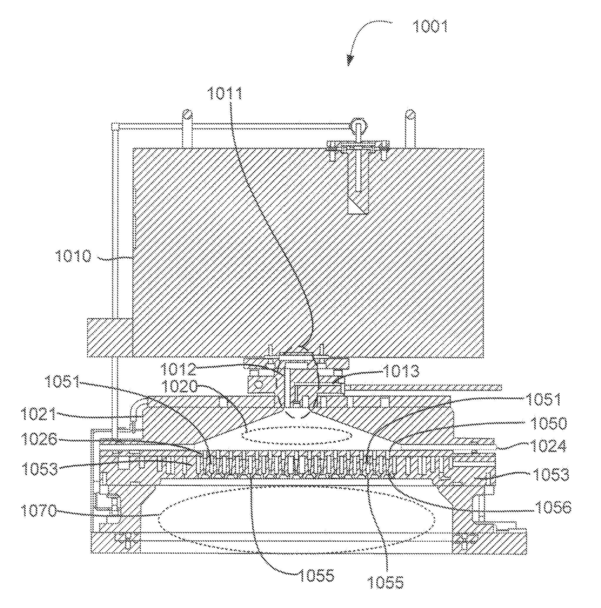
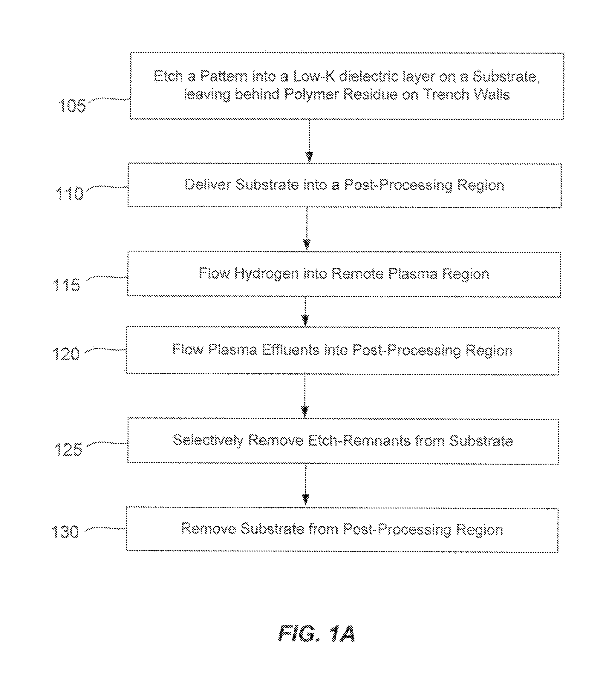
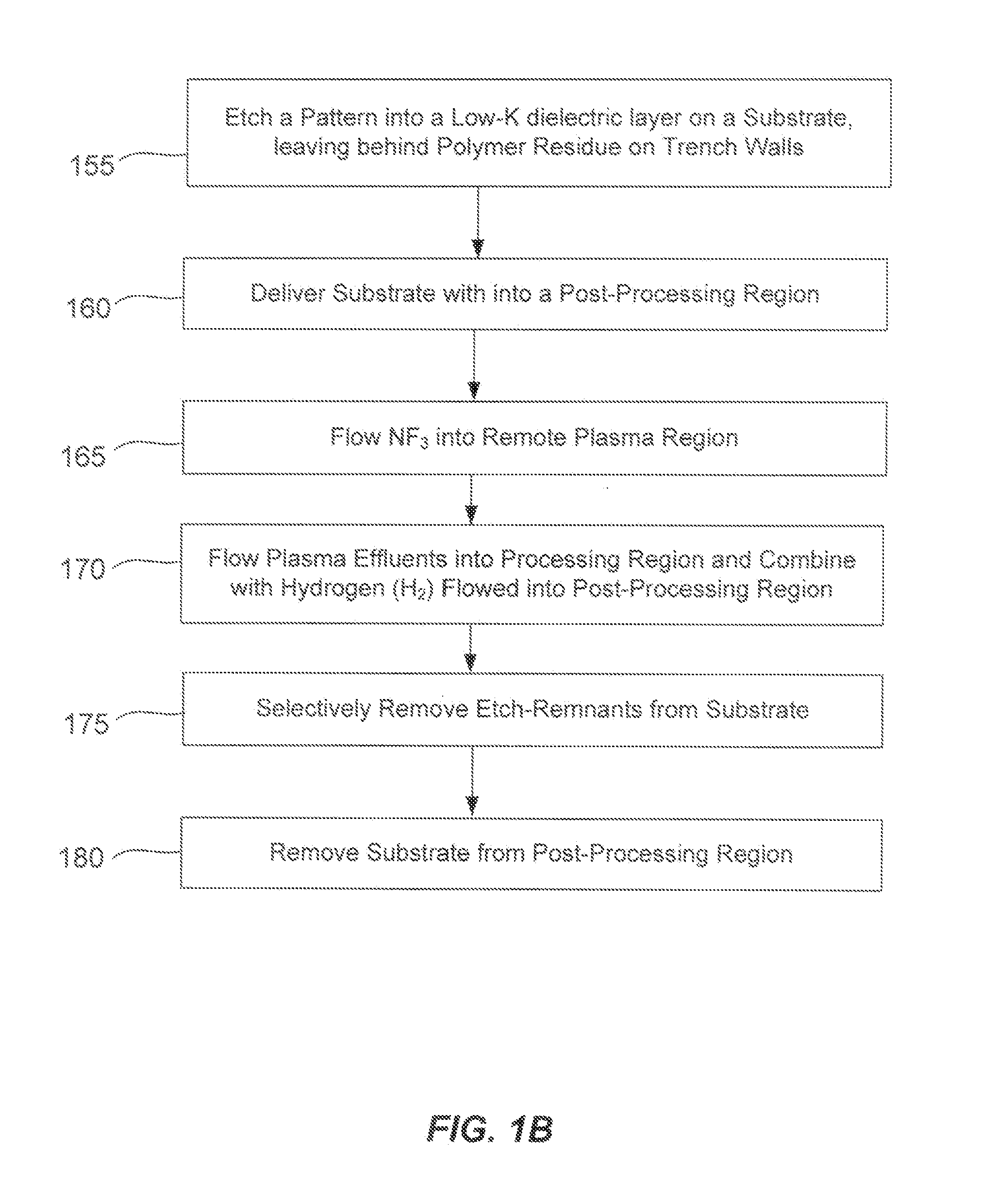
[0020]Methods of removing residual polymer from vertical walls of a patterned dielectric layer are described. The methods involve the use of a gas phase etch to remove the residual polymer without substantially disturbing the patterned dielectric layer. The gas phase etch may be used on a patterned low-k dielectric layer and may maintain the low dielectric constant of the patterned dielectric layer. The gas phase etch may further avoid stressing the patterned low-k dielectric layer by avoiding the use of liquid etchants whose surface tension can upset delicate low-K features. The gas phase etch may further avoid the formation of solid etch by-products which can also deform the delicate features.
[0021]Many dielectric etch processes use concurrent polymer deposits on the sidewalls of trenches to ensure the formation of more-or-less vertical sidewalls. Forming trenches in low-K dielectric layers tends to be more complex than forming trenches in high-K dielectrics. Low-K. dielectric lay...
PUM
| Property | Measurement | Unit |
|---|---|---|
| dielectric constant | aaaaa | aaaaa |
| temperature | aaaaa | aaaaa |
| temperature | aaaaa | aaaaa |
Abstract
Description
Claims
Application Information