Display device

a technology of display panel and display panel, which is applied in the direction of display/control unit casings, instruments, and electrical apparatus casings/cabinets/drawers, etc., can solve the problems of reducing contrast, affecting the appearance of the display panel, so as to reduce the thickness of the adhesive material between the display panel and the front window, prevent the effect of substrate deformation due to cure shrinkage and reduce the thickness of the adhesive material

Active Publication Date: 2013-11-14
JAPAN DISPLAY INC
View PDF2 Cites 29 Cited by
  • Summary
  • Abstract
  • Description
  • Claims
  • Application Information

AI Technical Summary

Benefits of technology

[0010]FIG. 7 is a cross-sectional view showing a vicinity of a display portion of a liquid crystal display device using a front window 10. In FIG. 7, a liquid crystal display panel 2 includes a TFT substrate 100, an opposing substrate 200, a lower polarizing plate 110, and an upper polarizing plate 210. The front window 10 is bonded onto the upper polarizing plate 210 with an adhesive material 50 curable by irradiation of an ultraviolet ray (hereinafter, UV adhesive material). Black light-blocking printing 12 is applied around the front window 10. However, such light-blocking printing 12 alone cannot block the stray light from the backlight or the like via the front window 10, allowing the light to enter the display area through the periphery of the front window 10, resulting in degradation of contrast.
[0015]If such a thick adhesive material layer 50 is formed, it means that a large amount of the UV material 50 is used. To use a large amount of the UV adhesive material 50, the UV adhesive material 50 must be applied to both sides of the front window 10 and the liquid crystal display panel 2 for bonding, which requires not only a high material cost but also a high production cost. Furthermore, the large amount of the adhesive material 50 may cause more stress due to cure shrinkage of the UV adhesive material 50, leading to a warpage problem of the opposing substrate 200 in the liquid crystal display panel 2. Moreover, a small thickness of the adhesive material 50 may cause another problem that a bubble in the adhesive material layer 50 can hardly escape.
[0021]An object of the present invention is, as described above, to prevent the phenomenon that the thickness of the adhesive material 50 between the liquid crystal display panel 2 and the front window 10 is increased and the occurrence of the white line around the display area due to the stray light from the side of the front window 10, in the liquid crystal display device employing both the upper frame 30 and the front window 10.
[0028]According to the present invention, because the thickness of the adhesive material between the front window and the display panel can be smaller than the thickness of the adhesive material between the upper fame covering the periphery of the display panel and the front window, the extrusion of the adhesive material can be reduced. Thus, there is no need of increasing the size of the lower chamfer of the front window, and the white line around the screen due to the stray light from the lower chamfer of the front window can be prevented.
[0029]Furthermore, because the thickness of the adhesive material between the display panel and the front window can be reduced, deformation of the substrate due to the cure shrinkage can be prevented.
[0030]Moreover, because the thickness of the adhesive material between the display panel and the front window can be reduced, the material cost can be reduced and workability can be improved. In addition, the bubble in the adhesive material can easily escape to the outside.

Problems solved by technology

However, it is difficult to completely shield such stray light.
With the liquid crystal display device using the front window, such stray light entering through a side face of the front window from the backlight and the like has become problematic.
However, such light-blocking printing 12 alone cannot block the stray light from the backlight or the like via the front window 10, allowing the light to enter the display area through the periphery of the front window 10, resulting in degradation of contrast.

Method used


Image

  • Display device
  • Display device
  • Display device

Examples


first embodiment

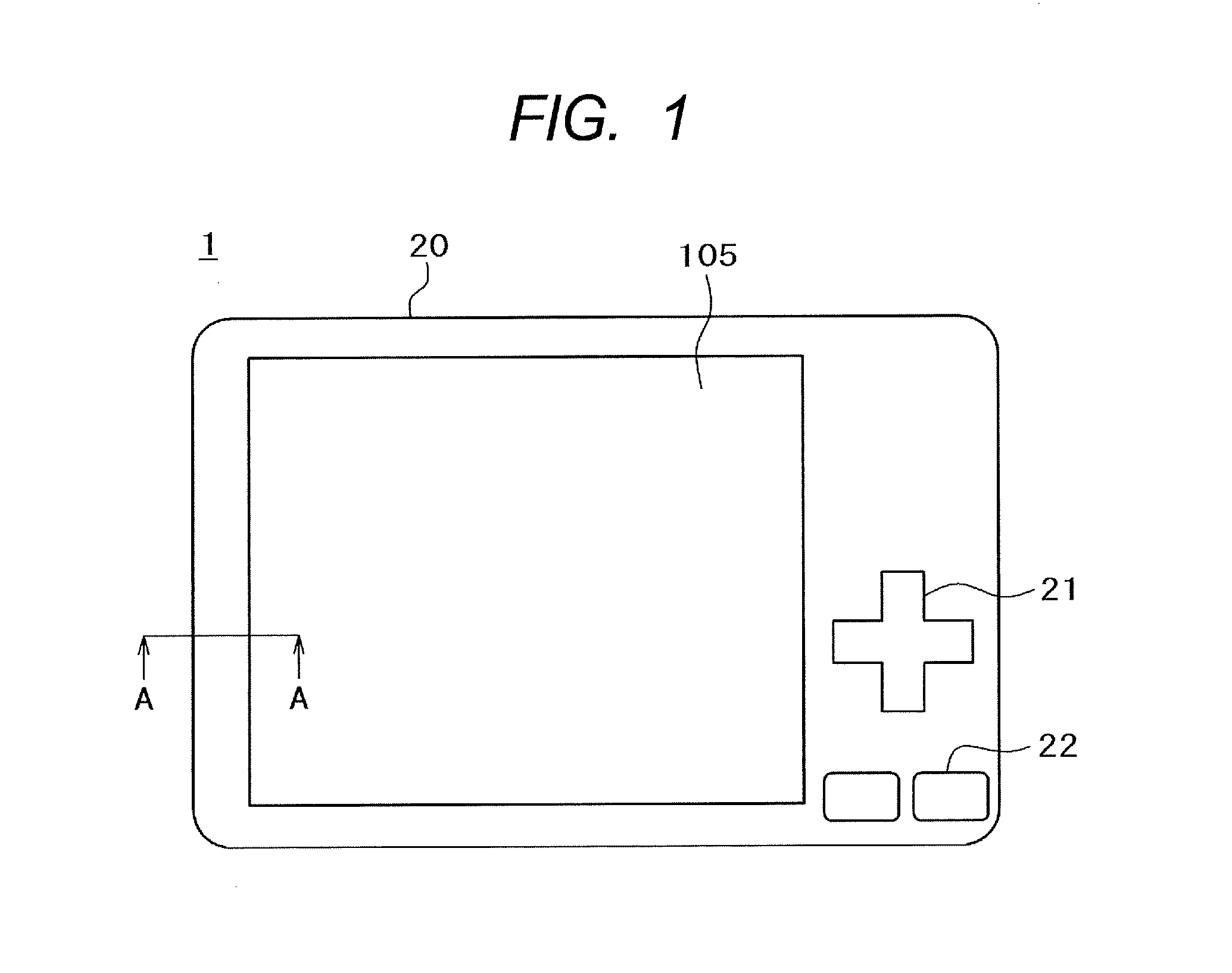
[0040]FIG. 1 is a plan view of a DSC 1 as an example to which the present invention can be applied. It is needless to say that the present invention can be applied not only to the DSC 1 but also to other displays. In FIG. 1, a control button 21, a switch button 22, and the like are arranged on the right side of a display area 105. Because the DSC 1 has an increased number of pixels and a high image quality is required, it is required to exhibit a high contrast even in the periphery of the display area 105.

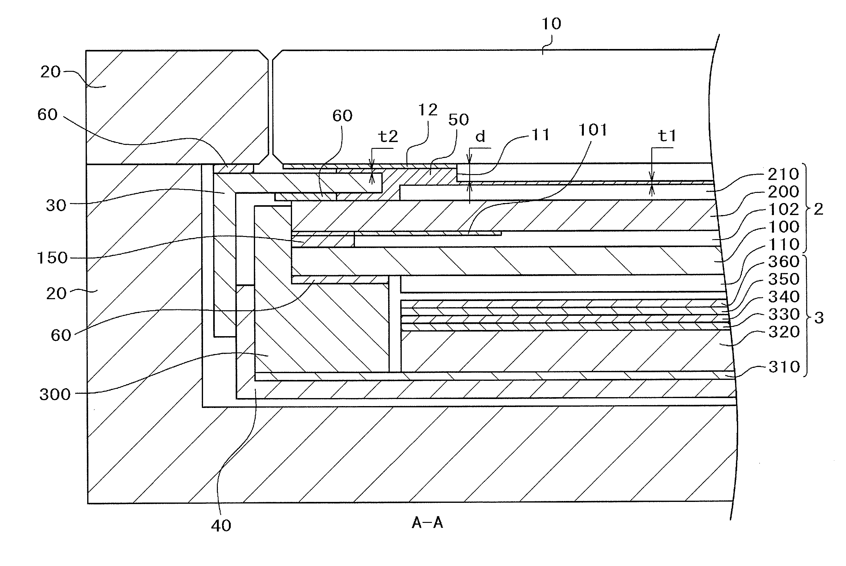
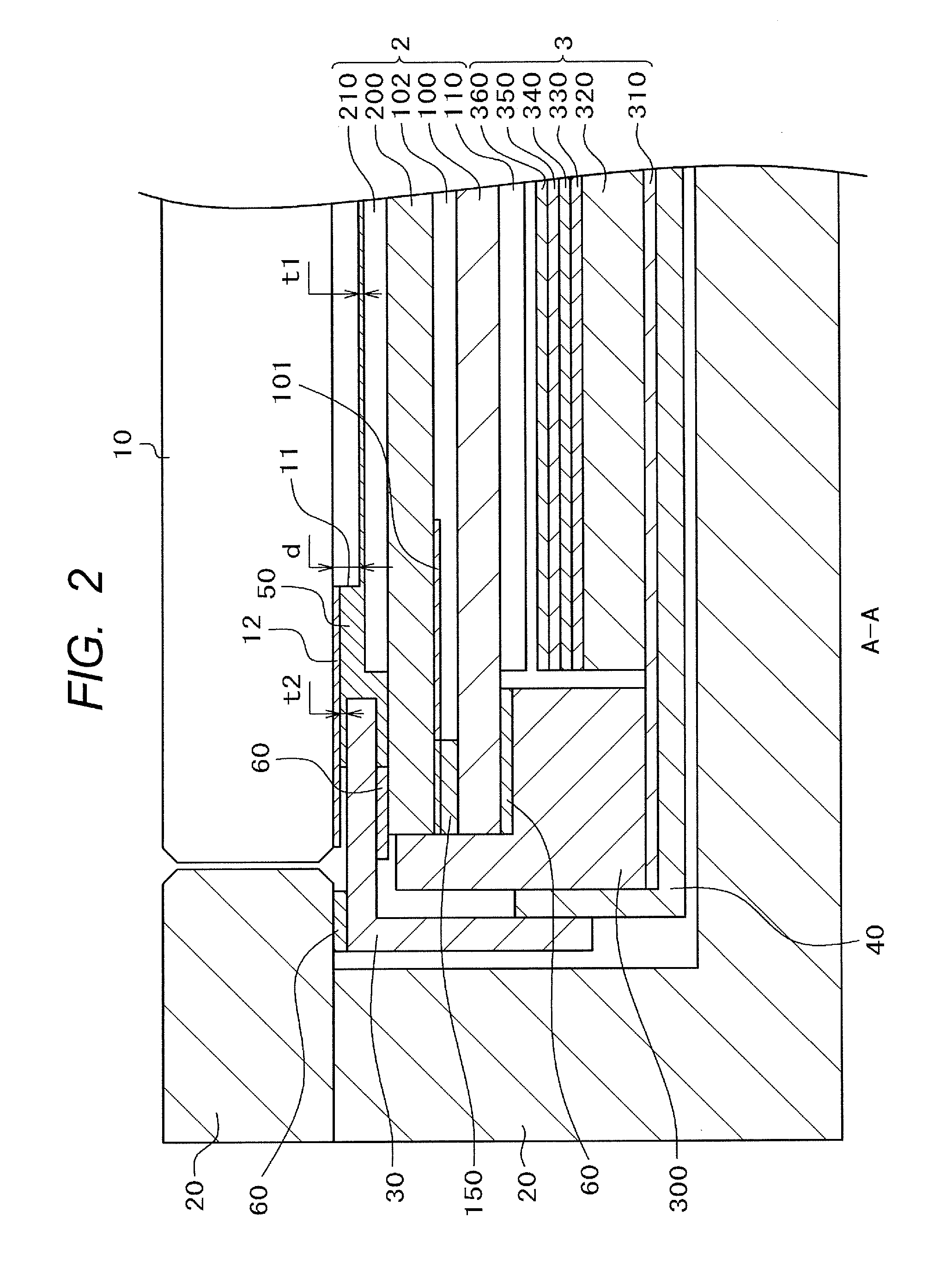
[0041]FIG. 2 is an A-A cross-sectional view of FIG. 1 showing a feature of the present invention. In FIG. 2, a liquid crystal display panel 2 has a configuration described below. Namely, a liquid crystal layer 102 is sandwiched between a TFT substrate 100 including a TFT and a pixel electrode arranged in a matrix form and an opposing substrate 200 formed thereon with a color filter and the like, a lower polarizing plate 110 is bonded to a lower side of the TFT substrate 100, and an...

second embodiment

[0054]Although the present invention was described in association with an application to the liquid crystal display device in the first embodiment, the present invention is not limited to the liquid crystal display device but can also be applied to an organic EL display device. The organic EL display device has a light emitting display area, and therefore it does not require a backlight. However, even in the case of such a light emitting device, there can be stray light in the front window.

[0055]FIG. 6 is a schematic cross-sectional view of an organic EL display panel 4. In FIG. 6, an organic EL layer 420 is formed on an element substrate 400, and an image is formed by the organic EL layer 420 emitting light upon receipt of a video signal. Because brightness of the organic EL layer 420 may be deteriorated by moisture, it is generally covered by a sealing substrate 410 made of glass to prevent the moisture in an atmosphere from entering. The element substrate 400 and the sealing subs...


PUM

PropertyMeasurementUnit
thicknessaaaaaaaaaa
thicknessaaaaaaaaaa
thicknessaaaaaaaaaa

Abstract

An upper frame covers a periphery of a liquid crystal display panel, and a cover plate is bonded onto the upper frame and an upper polarizing plate of the liquid crystal display panel. A step is formed on the cover plate in a portion where the upper frame is bonded to the cover plate. This can reduce a thickness of resin between the upper polarizing plate and the cover plate, thereby reducing an extrusion of the resin into between the cover plate and the upper frame. Thus, a chamfer on a lower side of the cover plate can be reduced in size, and stray light from the lower side of the cover plate can be prevented. This can prevent a white line around a screen.

Description

CLAIM OF PRIORITY[0001]The present application claims priority from Japanese Patent Application JP 2012-107691 filed on May 9, 2012, the content of which is hereby incorporated by reference into this application.BACKGROUND OF THE INVENTION[0002]1. Field of the Invention[0003]The present invention relates to a display device, and specifically to a display device inhibiting a white line that may occur in a periphery of a display area in a configuration where a frame and a front window (a cover plate) are arranged on a display panel.[0004]2. Background Art[0005]A liquid crystal display device is provided with a TFT substrate including a pixel electrode and a thin film transistor (TFT) in a matrix form and an opposing substrate opposing the TFT substrate and formed thereon with a color filter or the like in a position corresponding to the pixel electrode of the TFT substrate, and liquid crystal is sandwiched between the TFT substrate and the opposing substrate. The device forms an image...

Claims


Application Information

Patent Timeline
Patent Type & Authority Applications(United States)
IPC IPC(8): H05K5/00H05B33/02G02F1/1333
CPCH05K5/0017G02B1/105H05B33/02G02F1/133308G02F2202/28G02F1/13332G02F1/133331
Inventor SUZUKI, YUUJI
Owner JAPAN DISPLAY INC
Why Eureka
Try Eureka