Apparatus and Method for Microfabricated Multi-Dimensional Sensors and Sensing Systems

a multi-dimensional sensor and sensor technology, applied in the field of microfabricated devices, can solve the problems of not all devices can implement unique operating protocols and smart algorithms, not all sensors of the tcd or chemiresistor type have sufficient low power to work effectively, etc., to achieve low power, high production volume, and low power

Active Publication Date: 2013-11-21
SENSIRION AG
View PDF5 Cites 33 Cited by
  • Summary
  • Abstract
  • Description
  • Claims
  • Application Information

AI Technical Summary

Benefits of technology

[0017]The apparatus and methods for manufacturing nano-sensor platforms are advantageous for environmental, health, process, and safety monitoring of fluids, especially small molecule gases. It can now be seen that the many different functionalization layers of the same MEMS platform provides for an almost boundless number of sensors and sensor arrays that contain homogenous and/or heterogeneous layers on the exact same MEMS prepared platform with a wide variety of sensing reactions and reactivity. Not only can many sensors be arrayed on a single surface but the present invention allows diverse and different classes of sensors and related devices like pre-concentrators to be prepared on the same substrate with no change to the underlying platform but only a change in the selection of the functionalization layer(s) in the final processing steps. The surprising number of orthogonally reactive sensors and sensor classes on the same platform constitute a new and more powerful sensing capability. In addition to the surprisingly more effective sensing, the new platform allows designs that are ultra low power for portability, versatility, and interface with modern wireless systems for the underlying platform [e.g., leading to potentially higher production volumes] making MEMS fabrication of chemical sensors practical for real-world applications that are low volume, while heretofore only high volume applications were economically possible and commercially viable using MEMS. There are many additional couplings of this technology to the world of sensing such as thermal isolation techniques to achieve lower power, the use of the ever increasing number of possible materials including plastics and composites, flexible circuit materials for construction, and alternative selective and non-selective functionalization layers for use in liquids and gases. Some

Problems solved by technology

However, not all combinations of the materials and processes result in an element or device which possesses the surprising combined properties of sensor performance for practical application in modern low power low cost situations and applications.
And not all devices can implement the unique operating protocols and smart algo

Method used


Image

  • Apparatus and Method for Microfabricated Multi-Dimensional Sensors and Sensing Systems
  • Apparatus and Method for Microfabricated Multi-Dimensional Sensors and Sensing Systems
  • Apparatus and Method for Microfabricated Multi-Dimensional Sensors and Sensing Systems

Examples


Embodiment Construction

[0066]Reference will now be made in detail to various embodiments which are illustrated in the accompanying drawings, wherein like numerals indicate similar elements throughout the views.

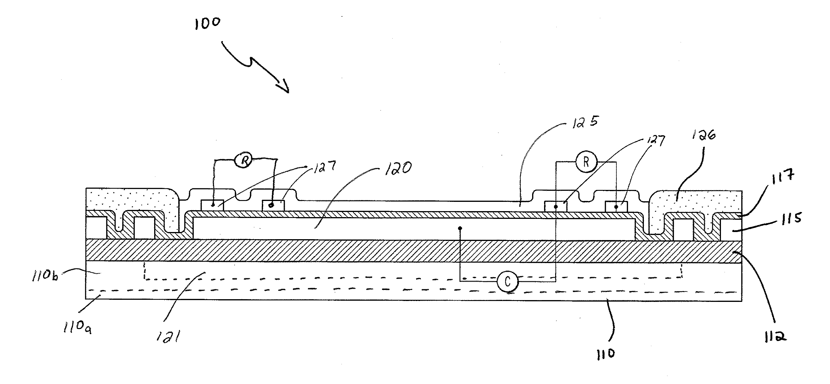
[0067]One embodiment of the present invention is the development of microfabricated sensors that can detect critical fluids, especially small molecule gases. Putting this technology into a low-cost MEMS package can add to the unique character of the resulting sensors. These MEMS sensors will be unique because of the combination of high-technological performance, tiny size, low power and low cost and the potential for long lifetime and exceptional stability (which is unique for chemical sensors and significantly increases the ability of these chemical sensors to be part of modern wired and wireless sensing systems).

[0068]Described below in varying embodiments are unobtrusive, small, lightweight and energy efficient monitoring devices combining communication equipment and various sensors for detection...


PUM


Abstract

A universal microelectromechanical (MEMS) nano-sensor platform having a substrate and conductive layer deposited in a pattern on the surface to make several devices at the same time, a patterned insulation layer, wherein the insulation layer is configured to expose one or more portions of the conductive layer, and one or more functionalization layers deposited on the exposed portions of the conductive layer to make multiple sensing capability on a single MEMS fabricated device. The functionalization layers are adapted to provide one or more transducer sensor classes selected from the group consisting of: radiant, electrochemical, electronic, mechanical, magnetic, and thermal sensors for chemical and physical variables and producing more than one type of sensor for one or more significant parameters that need to be monitored.

Description

CROSS-REFERENCE TO RELATED APPLICATIONS[0001]This application is a continuation-in-part application of copending U.S. Non-Provisional patent application Ser. No. 13 / 271,659, filed Oct. 10, 2011, which is a continuation-in-part application of U.S. Non-Provisional patent application Ser. No. 12 / 615,110, filed Nov. 9, 2009, now granted as U.S. Pat. No. 8,310,016, which is a continuation-in-part application of U.S. Non-Provisional patent application Ser. No. 11 / 879,462, filed Jul. 17, 2007, now granted as U.S. Pat. No. 7,911,010, the entire disclosures of which are hereby incorporated by reference herein. This application also claims priority from U.S. Provisional Patent Application Ser. No. 61 / 112,237, filed Nov. 7, 2008, and U.S. Provisional Patent Application Ser. No. 61 / 392,217, filed Oct. 12, 2010, the entire disclosures of which are hereby incorporated by reference herein.STATEMENT REGARDING FEDERALLY SPONSORED RESEARCH OR DEVELOPMENT[0002]This invention was made with government s...

Claims


Application Information

Patent Timeline
IPC IPC(8): G01N27/00
CPCG01N27/00A61B5/0205A61B5/021A61B5/024A61B5/0816A61B5/14551A61B2560/0242A61B2562/028G01N27/128G01N33/005
Inventor STETTER, JOSEPH R.SHIRKE, AMOL G.
Owner SENSIRION AG
Why Eureka
Try Eureka