Wrap-around fin for contacting a capacitor strap of a dram

Inactive Publication Date: 2013-12-05
GLOBALFOUNDRIES INC
View PDF6 Cites 19 Cited by
  • Summary
  • Abstract
  • Description
  • Claims
  • Application Information

AI Technical Summary

Problems solved by technology

As dimensions of semiconductor devices scale, providing a robust low resistance path for electrical conduction between an inner electrode of a transistor and the source of an access transistor becomes a challenge because available area for forming a conductive strap structure decreases.

Method used


Image

  • Wrap-around fin for contacting a capacitor strap of a dram
  • Wrap-around fin for contacting a capacitor strap of a dram
  • Wrap-around fin for contacting a capacitor strap of a dram

Examples


first embodiment

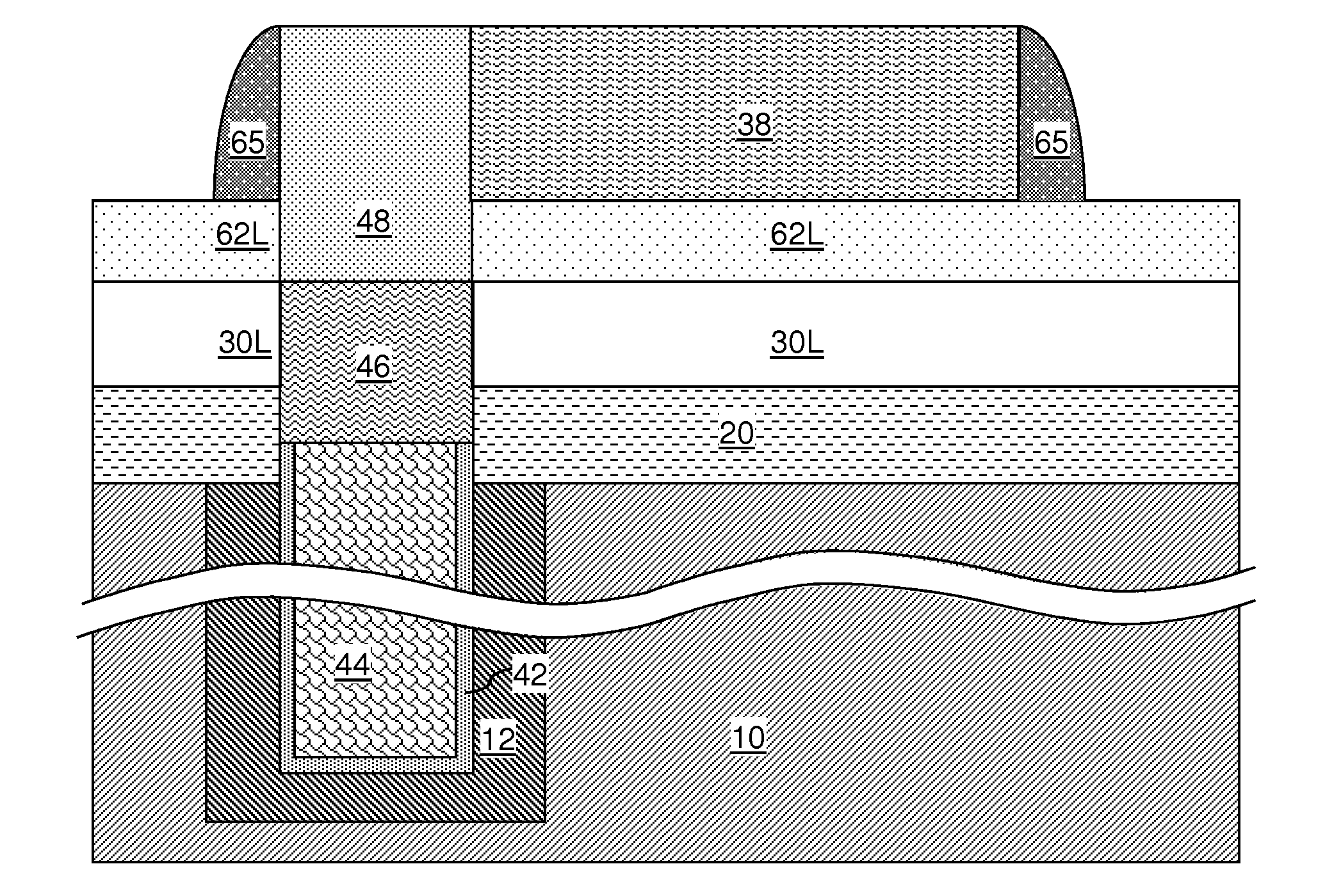
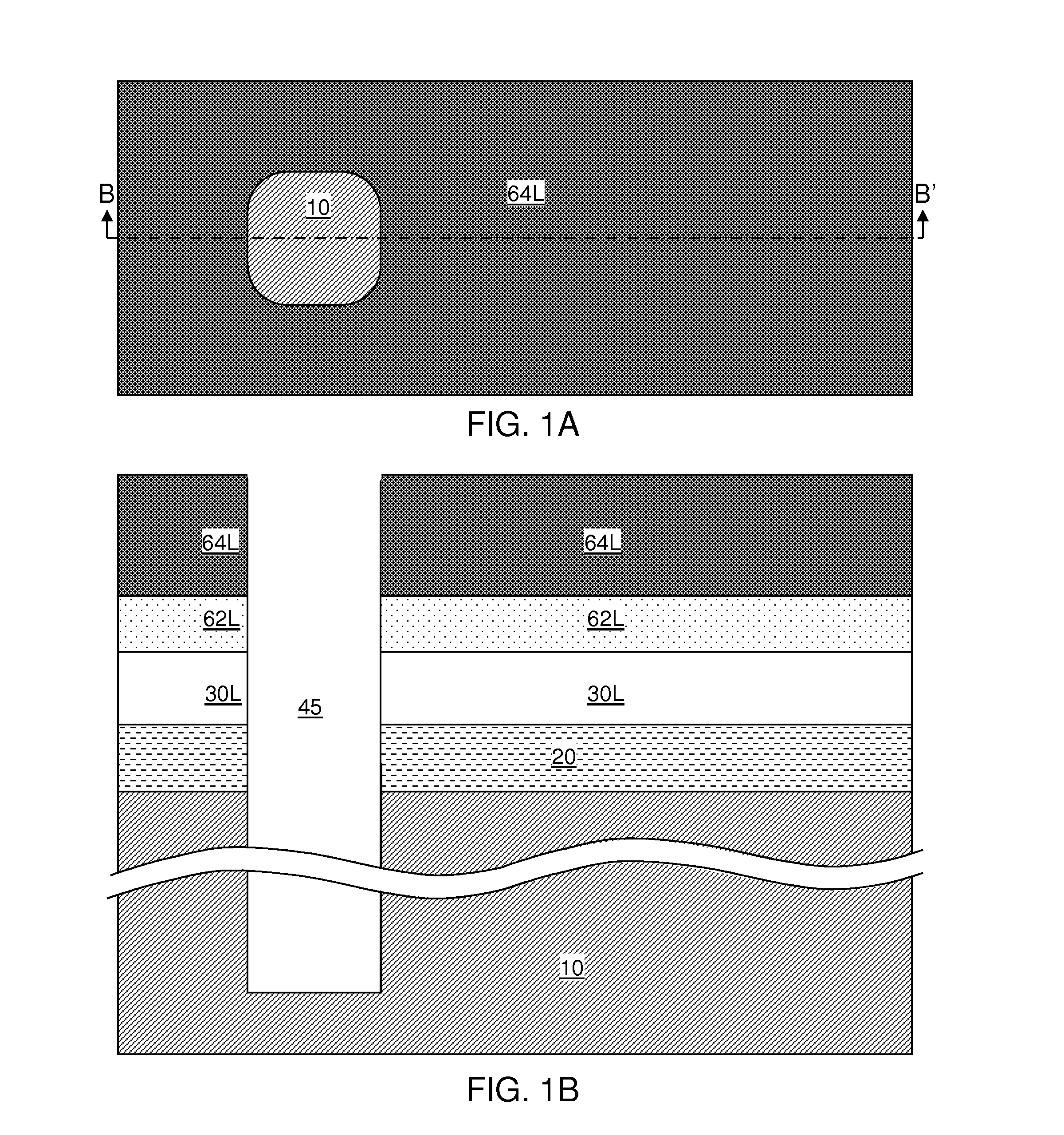
[0083]Referring to FIGS. 1A and 1B, a first exemplary semiconductor structure according to the present disclosure includes a semiconductor-on-insulator (SOI) substrate. The SOI substrate includes a stack, from bottom to top, of a bottom semiconductor layer 10, a buried insulator layer 20, and a top semiconductor layer 30L.

[0084]The bottom semiconductor layer 10 includes a semiconductor material. The buried insulator layer 20 includes a dielectric material such as silicon oxide, silicon nitride, a dielectric metal oxide, or a combination thereof. The top semiconductor layer 30L includes a semiconductor material, which can be the same as, or different from, the semiconductor material of the bottom semiconductor layer 10.

[0085]Each of the bottom semiconductor layer 10 and the top semiconductor layer 30L includes a semiconductor material independently selected from elemental semiconductor materials (e.g., silicon, germanium, carbon, or alloys thereof), III-V semiconductor materials, or ...

second embodiment

[0139]Referring to FIGS. 19A and 19B, a second exemplary semiconductor structure according to the present disclosure can be formed employing the same processing steps of the first exemplary semiconductor structure, and by modifying the pattern for various elements in the first exemplary semiconductor structure. Specifically, a pair of deep trench capacitors is formed, and the mask material portion 38 is patterned to extend between two dielectric capacitor caps 48. The two linear portions of the semiconductor fin 30 laterally extend between the two dielectric capacitor caps 48. The semiconductor fin 30 is formed as a structure homeomorphic to a torus, and laterally surrounds, and contacts, two conductive strap structures 46. A pair of drain regions 36 laterally separated by the same distance as two pairs of channel regions 32 are formed within the semiconductor fin. Two access transistors share the pair of drain regions 36. While each access transistor is a trigate finFET, a variatio...


PUM


Abstract

A conductive strap structure in lateral contact with a top semiconductor layer is formed on an inner electrode of a deep trench capacitor. A cavity overlying the conductive strap structure is filled a dielectric material to form a dielectric capacitor cap having a top surface that is coplanar with a topmost surface of an upper pad layer. A semiconductor mandrel in lateral contact with the dielectric capacitor cap is formed. The combination of the dielectric capacitor cap and the semiconductor mandrel is employed as a protruding structure around which a fin-defining spacer is formed. The semiconductor mandrel is removed, and the fin-defining spacer is employed as an etch mask in an etch process that etches a lower pad layer and the top semiconductor layer to form a semiconductor fin that laterally wraps around the conductive strap structure. An access finFET is formed employing two parallel portions of the semiconductor fin.

Description

BACKGROUND[0001]The present disclosure relates to a semiconductor structure, and particularly to a dynamic random access memory (DRAM) cell including a finFET access transistor and a method of manufacturing the same.[0002]Deep trench capacitors are used in a variety of semiconductor chips for high areal capacitance and low device leakage. Typically, a deep trench capacitor provides a capacitance in the range from 4 fF (femto-Farad) to 120 fF. A deep trench capacitor may be employed as a charge storage unit in a dynamic random access memory (DRAM), which may be provided as a stand-alone semiconductor chip, or may be embedded in a system-on-chip (SoC) semiconductor chip. A deep trench capacitor may also be employed in a variety of circuit applications such as a charge pump or a capacitive analog component in a radio-frequency (RF) circuit.[0003]As dimensions of semiconductor devices scale, providing a robust low resistance path for electrical conduction between an inner electrode of a...

Claims


Application Information

Patent Timeline
Patent Type & Authority Applications(United States)
IPC IPC(8): H01L27/108H01L21/8242
CPCH01L27/1207H01L27/1211H10B12/36H10B12/37H10B12/0385H10B12/056
Inventor BEAUDOIN, FELIXLUCARINI, STEPHEN M.WANG, XINHUIWANG, XINLIN
Owner GLOBALFOUNDRIES INC
Why Eureka
Try Eureka