

Method and structure providing optical isolation of a waveguide on a silicon-on-insulator substrate
a silicon-on-insulator substrate and optical isolation technology, applied in the direction of optical waveguide light guide, instruments, electrical equipment, etc., can solve the problems of unsatisfactory optical signal loss and lessen the effect of heat sink
- Summary
- Abstract
- Description
- Claims
- Application Information
AI Technical Summary
Benefits of technology
Problems solved by technology
Method used
Image

Examples
Embodiment Construction
[0010]In the following detailed description, reference is made to the accompanying drawings which form a part hereof, and in which is shown by way of illustration specific embodiments that may be practiced. These embodiments are described in sufficient detail to enable those skilled in the art to make and use them, and it is to be understood that structural, logical, or procedural changes may be made to the specific embodiments disclosed without departing from the spirit and scope of the invention.
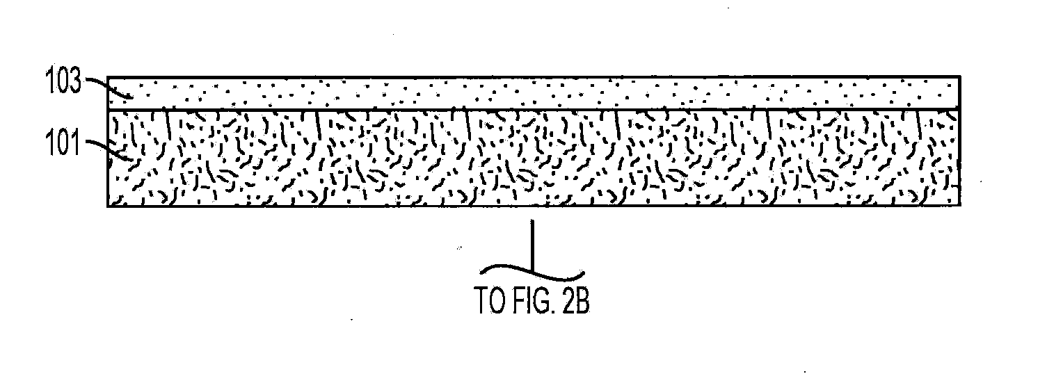
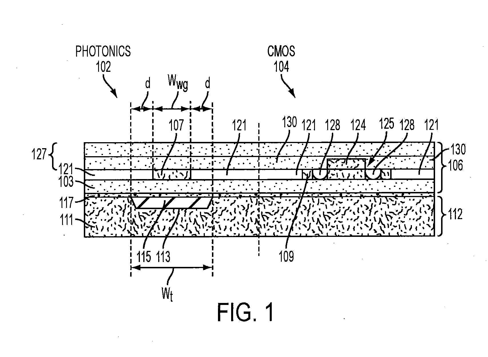
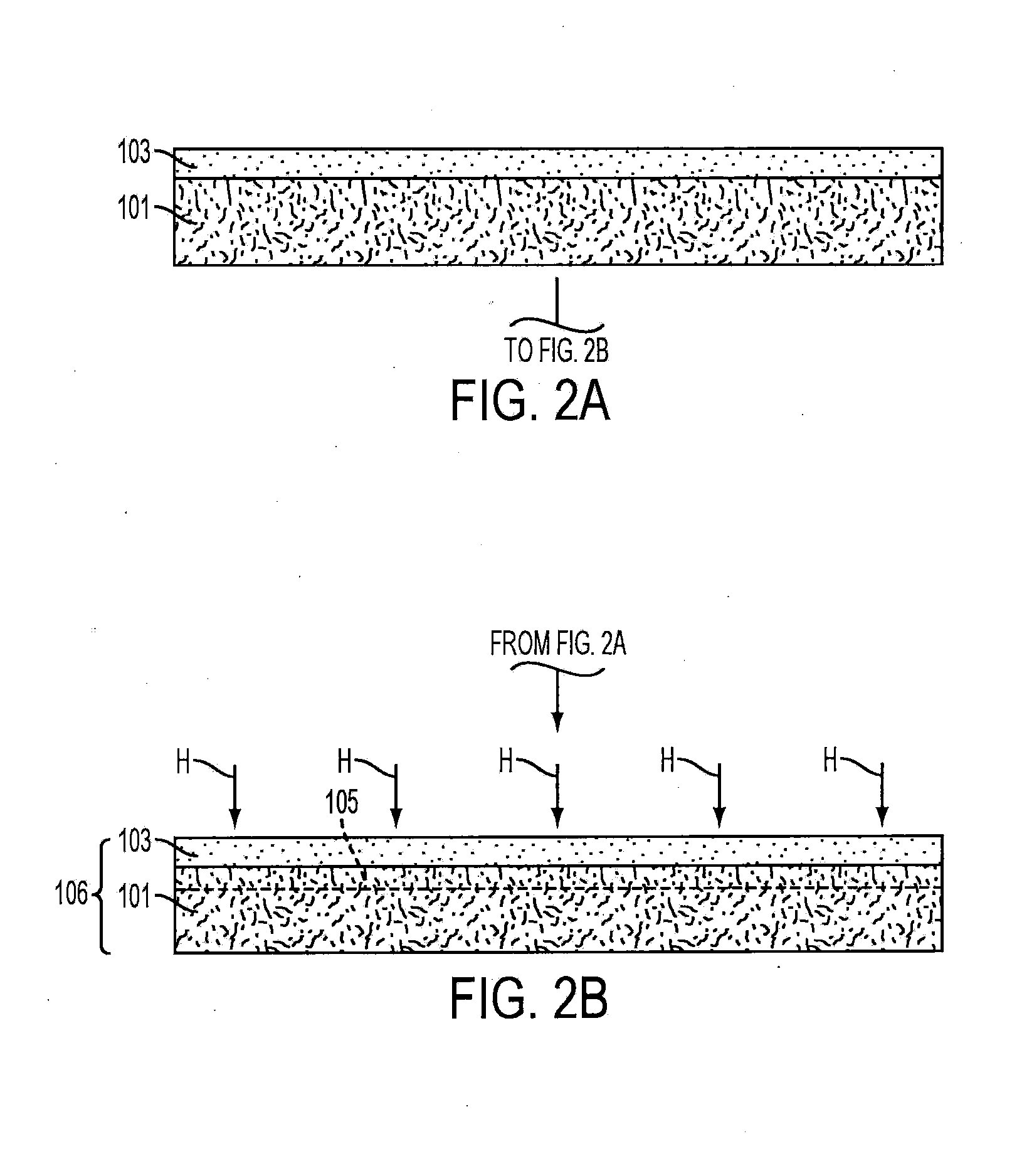
[0011]Embodiments described herein provide a silicon on insulator (SOI) structure on which both photonic devices and electronic circuits can be formed with a sufficient optical decoupling of the core of a waveguide from a first support substrate to prevent optical loss by evanescent coupling, while retaining good heat dissipation Optical decoupling is provided by a shallow trench isolation area formed in the first substrate which is beneath and extends along the waveguide core. When the fi...
PUM
 Abstract
Description
Claims
Application Information