Liquid crystal display panel and pixel array substrate thereof

a technology of liquid crystal display and substrate, applied in non-linear optics, instruments, optics, etc., can solve the problems of incessant development of har designs, and achieve the effect of improving the aperture ratio of high-resolution lcd panels

Inactive Publication Date: 2013-12-12
HANNSTAR DISPLAY CORPORATION
View PDF2 Cites 12 Cited by
  • Summary
  • Abstract
  • Description
  • Claims
  • Application Information

AI Technical Summary

Benefits of technology

[0020]In conclusion, In the LCD panel and the pixel array substrate thereof according to the present invention, the transparent conductive layer and the pixel electrode are uded to form a storage capacitor, so as to improve the aperture ratio of the high-resolution LCD panel. Furthermore, a capacity coupling effect on the pixel electrodes generated by components (the data lines, gate lines, thin film transistors, or a combination thereof), below the transparent conductive layer may also be prevented through the transparent conductive layer.

Problems solved by technology

Consequently, in the LCD technology, HAR designs still require incessant development.

Method used


Image

  • Liquid crystal display panel and pixel array substrate thereof
  • Liquid crystal display panel and pixel array substrate thereof
  • Liquid crystal display panel and pixel array substrate thereof

Examples


Embodiment Construction

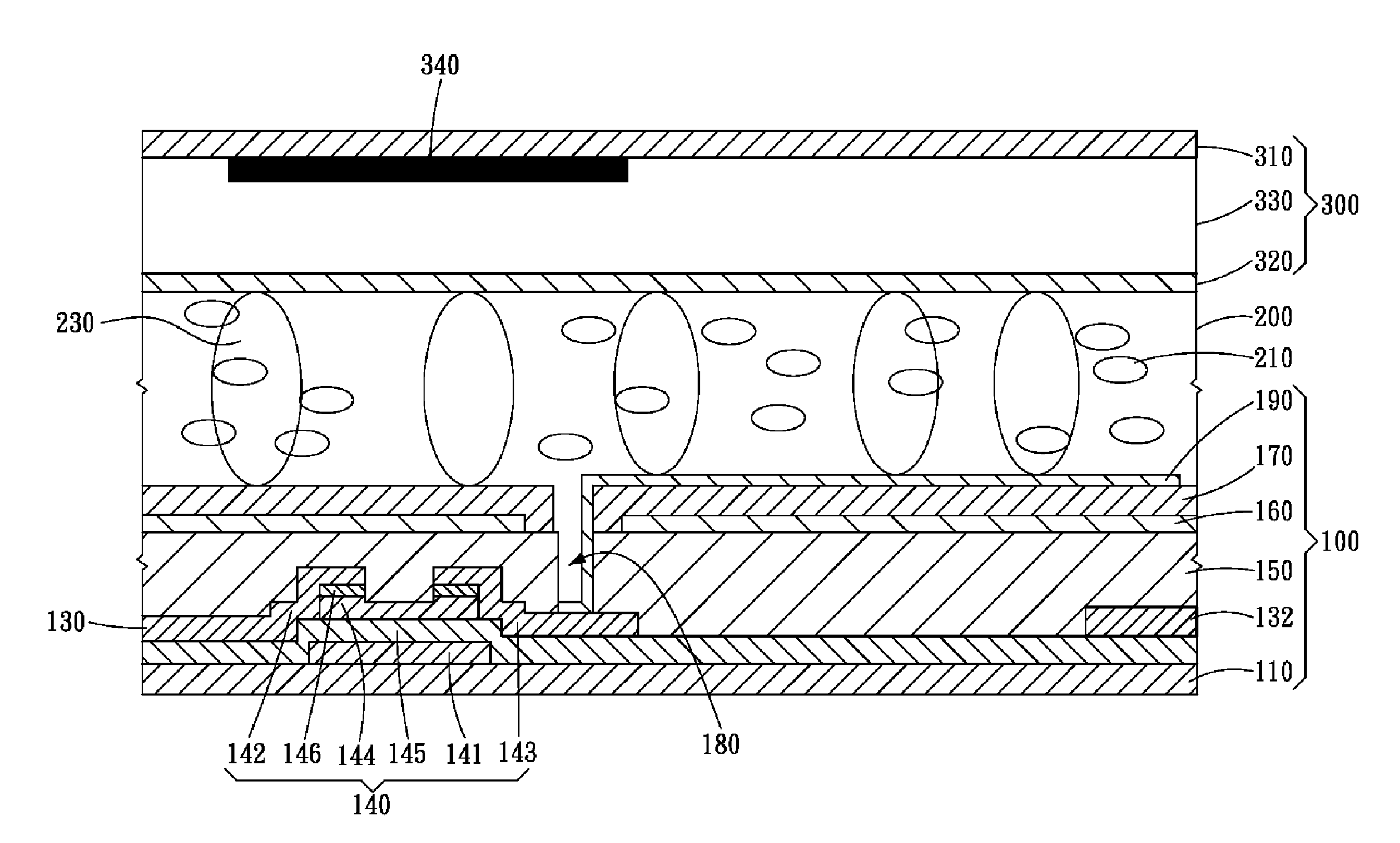
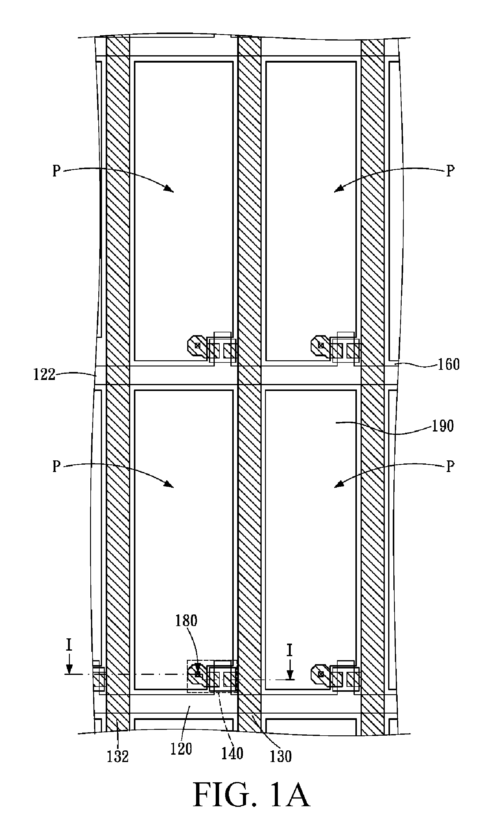
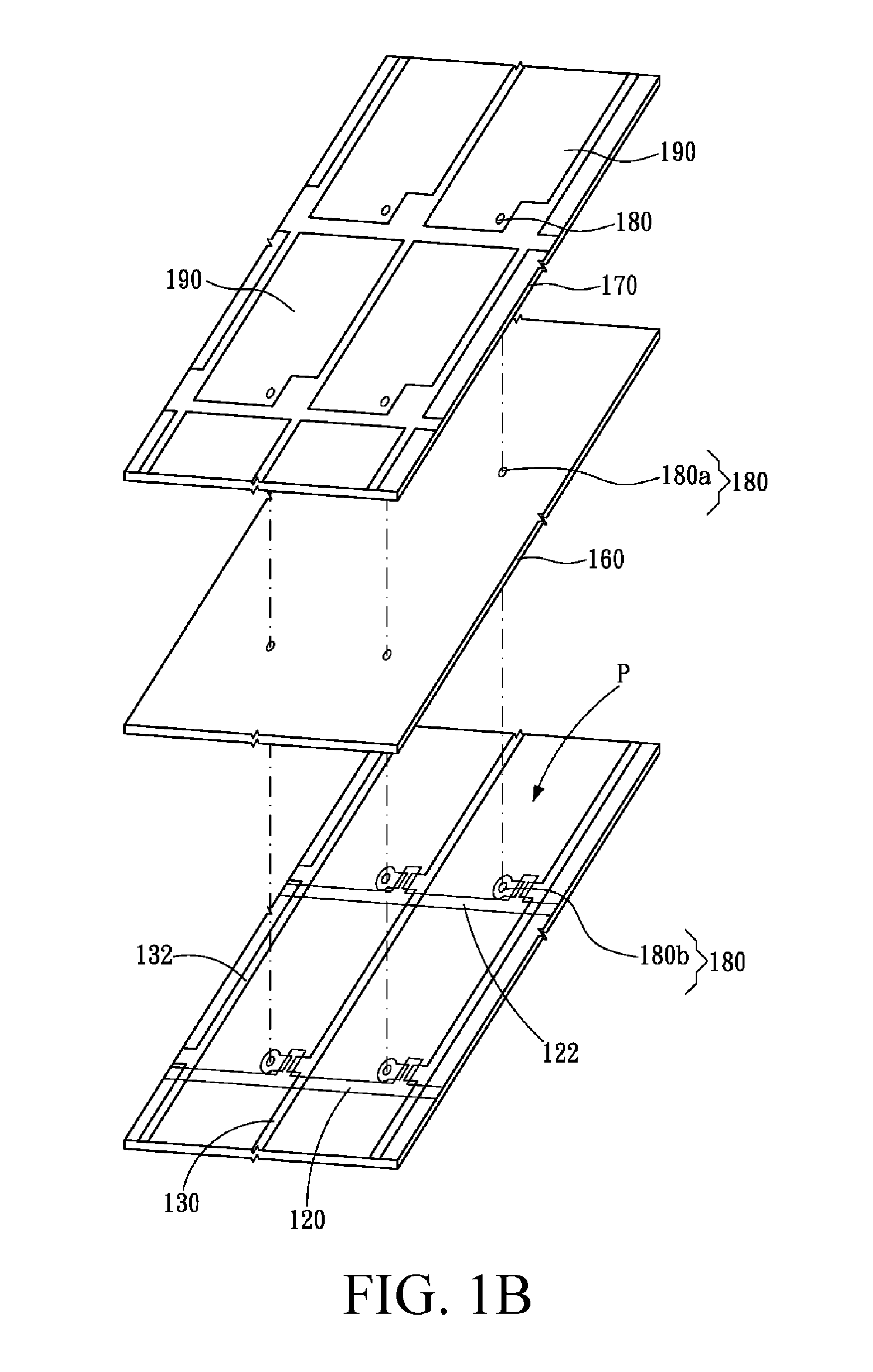
[0037]FIG. 1A is a top view of a pixel array substrate according to a first embodiment of the present invention. FIG. 1B is a schematic exploded view of the pixel array substrate shown in FIG. 1A. FIG. 1C is a sectional view along a line I-I of the pixel array substrate shown in FIG. 1A. For the convenience of description, insulation layers are omitted in the pixel array substrate shown in FIG. 1A.

[0038]Please refer to FIG. 1A, FIG. 1B and FIG. 1C, in which a pixel array substrate 100 includes a first substrate 110, a plurality of gate lines 120 and 122, a plurality of data lines 130 and 132, a plurality of thin film transistors 140, a first insulation layer 150, a transparent conductive layer 160, a second insulation layer 170, a plurality of contact holes 180 and a plurality of pixel electrodes 190.

[0039]The gate lines 120 and 122 and the data line 130 and 132 are disposed on the first substrate 110. The data lines 130 and 132 and the gate lines 120 and 122 are interlaced. Further...


PUM

PropertyMeasurementUnit
transparentaaaaaaaaaa
transmittanceaaaaaaaaaa
areasaaaaaaaaaa

Abstract

A liquid crystal display (LCD) panel and pixel array substrate thereof is related to the pixel array substrate including a first substrate, gate lines, data lines, thin film transistors, a first insulation layer, a transparent conductive layer, a second insulation layer, contact holes, and pixel electrodes. The gate lines, the data lines, and the thin film transistors are disposed on the first substrate, and the first insulation layer covers thereon. The transparent conductive layer is disposed on the first insulation layer and has a common voltage level. The second insulation layer is disposed between the transparent conductive layer and the pixel electrodes, and insulates the transparent conductive layer from the pixel electrodes. The pixel electrodes are coupled electrically to third terminals of the corresponding thin film transistors through the corresponding contact holes.

Description

CROSS-REFERENCES TO RELATED APPLICATIONS[0001]This non-provisional application claims priority under 35 U.S.C. §119(a) on Patent Application No. 201210193317.2 filed in China, P.R.C. on Jun. 12, 2012, the entire contents of which are hereby incorporated by reference.BACKGROUND[0002]1. Technical Field[0003]The present invention relates to a liquid crystal display (LCD) technology, and in particular, to an LCD panel and a pixel array substrate thereof.[0004]2. Related Art[0005]In recent years, flat-panel displays are developing more and more rapidly, and have gradually taken the place of conventional cathode-ray tube displays. Currently, the flat-panel displays are classified into the following types: an organic light-emitting diodes display (OLED), a plasma display panel (PDP), an LCD, and a field emission display (FED), and so on. The LCD technology can be classified into two modes according to the twisting manners of a liquid crystal molecular material. One is a twisted nematic LCD...

Claims


Application Information

Patent Timeline
Patent Type & Authority Applications(United States)
IPC IPC(8): G02F1/136
CPCG02F1/136213G02F1/136218
Inventor YU, CHIA-HUALIN, SUNG-CHUNLIU, HSUAN-CHEN
Owner HANNSTAR DISPLAY CORPORATION
Why Eureka
Try Eureka