Ceramic multilayer substrate and manufacturing method therefor

a multi-layer substrate and ceramic technology, applied in ceramic layered products, transportation and packaging, chemistry apparatus and processes, etc., can solve the problems of difficult to prevent the occurrence of sudden or unavoidable local oozing or spreading of a conductive paste, and high reliability, so as to reduce or prevent the occurrence of short-circuiting, improve the peel strength of surface electrodes, and improve the peel strength

Active Publication Date: 2013-12-12
MURATA MFG CO LTD
View PDF2 Cites 12 Cited by
  • Summary
  • Abstract
  • Description
  • Claims
  • Application Information

AI Technical Summary

Benefits of technology

[0022]With this configuration, a ceramic multilayer substrate having a structure in which the peripheral portion of a surface electrode is covered with a covering ceramic layer can be obtained. It is thus possible to manufacture a more highly reliable ceramic multilayer substrate in which, in addition to basic advantages of the preferred embodiments of the present invention, an advantage in improving the peel strength of surface electrodes can be obtained. The covering ceramic green layer which covers at least the peripheral portion of an electrode paste pattern, which defines a surface electrode, and does not cover the central portion of the electrode paste pattern may be formed by the following method, for example. A ceramic paste may be printed such that it covers at least the peripheral portion of an electrode paste pattern and does not cover the central portion of the electrode paste pattern. Alternatively, a ceramic green sheet including an opening from which the central portion of an electrode paste pattern, which forms a surface electrode, is exposed may be stacked.
[0023]The ceramic multilayer substrate according to a preferred embodiment of the present invention is a ceramic multilayer substrate including a ceramic substrate defined by a plurality of ceramic layers stacked on each other and electrodes disposed on or in the ceramic layer. A recessed portion is defined on a principal surface of any of the ceramic layers by the electrode and the surrounding ceramic layer. It is thus possible to significantly reduce or prevent the occurrence of short-circuiting between adjacent surface electrodes or adjacent internal electrodes, which would otherwise be caused by oozing or spreading of an electrode paste from an electrode.
[0024]As a result, it is possible to provide a highly reliable ceramic multilayer substrate, in which even if surface electrodes and internal electrodes are disposed at narrow intervals and at high density, short-circuiting between adjacent surface electrodes or between adjacent internal electrodes is significantly reduced or prevented.

Problems solved by technology

In such a ceramic multilayer substrate, as the size of the substrate becomes smaller, it is necessary that surface electrodes and internal electrodes be disposed at narrower intervals and at higher density, and thus, short-circuiting between adjacent surface electrodes or adjacent internal electrodes may likely to occur.
However, in the method disclosed in Japanese Unexamined Patent Application Publication No. 2003-151351, although it is possible to prevent oozing of a conductive paste from the entire pattern, which forms surface electrodes and internal electrodes formed by printing the conductive paste, it is difficult to prevent the occurrence of sudden or local oozing or spreading of a conductive paste from the surface electrodes and the internal electrodes.
Thus, the occurrence of local oozing or spreading of a conductive paste is unavoidable in some cases even if the conductive paste itself is changed.
Moreover, as a matter of fact, even if improvements in a print pattern or a printer are made, such local or sudden oozing or spreading of a conductive paste from surface electrodes and internal electrodes is unavoidable in some cases in a mass-production process.

Method used


Image

  • Ceramic multilayer substrate and manufacturing method therefor
  • Ceramic multilayer substrate and manufacturing method therefor
  • Ceramic multilayer substrate and manufacturing method therefor

Examples


first preferred embodiment

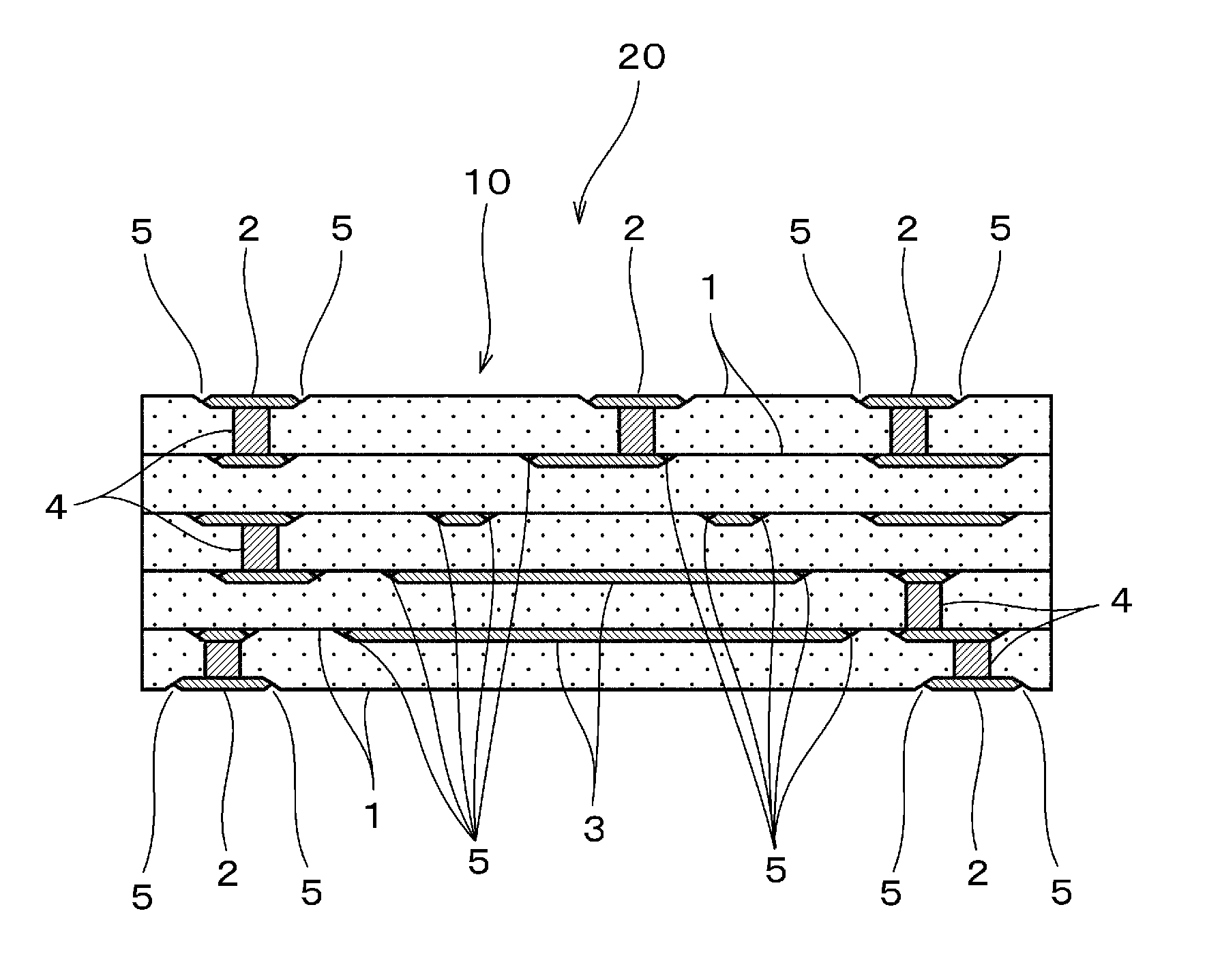
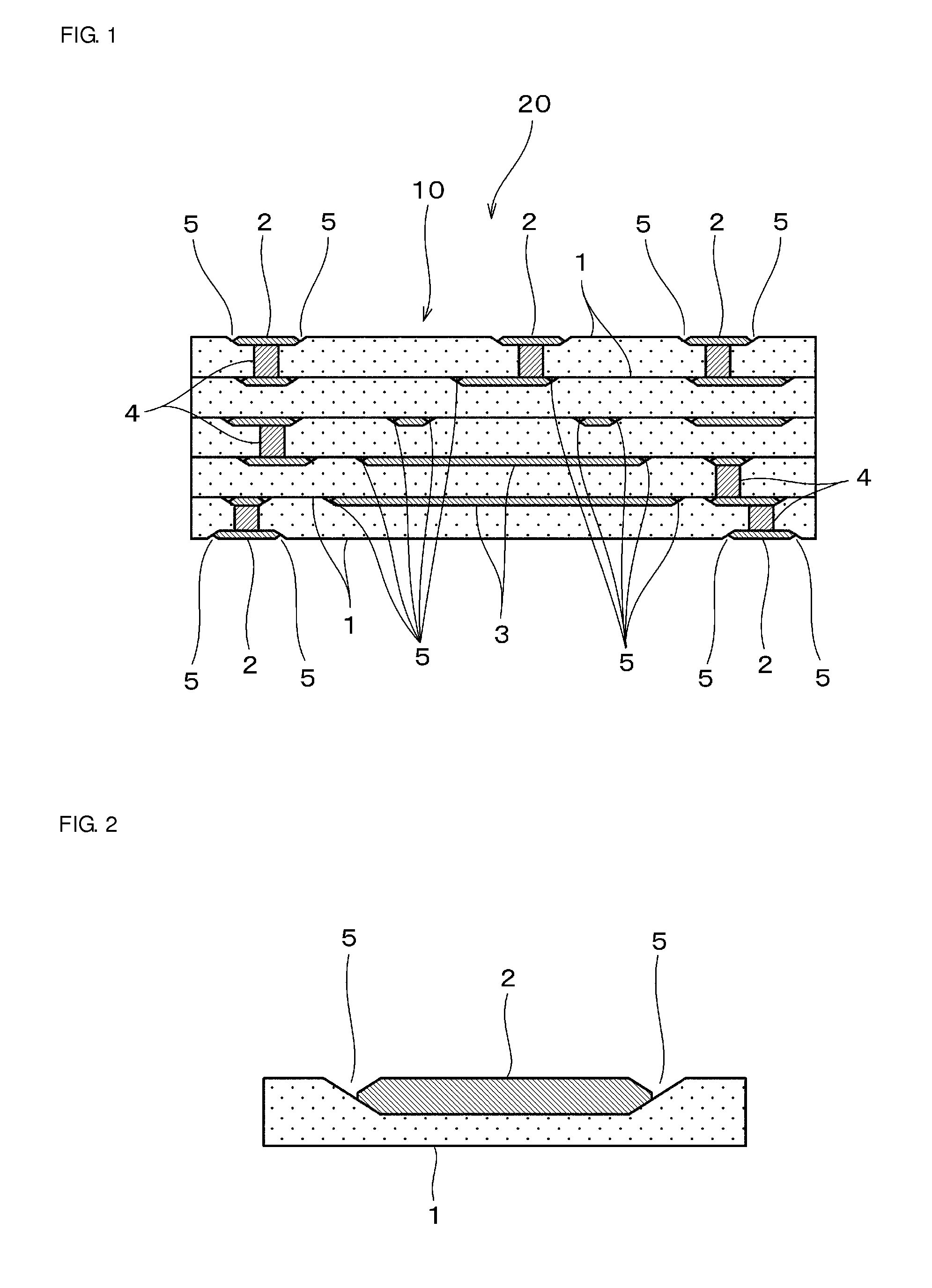
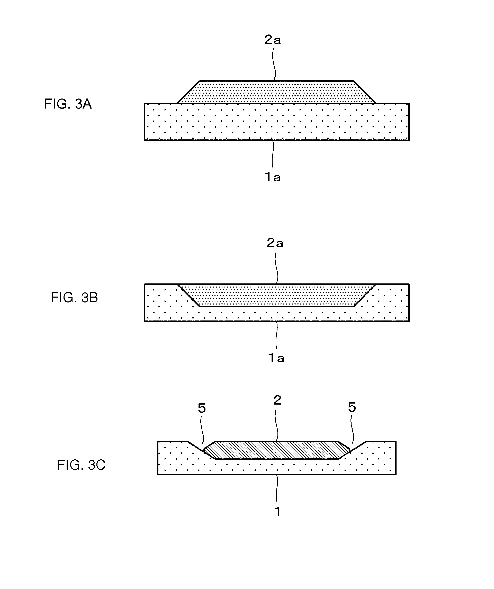
[0034]FIG. 1 is a sectional view schematically illustrating the entire configuration of a ceramic multilayer substrate 20 according to a first preferred embodiment of the present invention. FIG. 2 is a sectional view illustrating a portion of the ceramic multilayer substrate 20.

[0035]The ceramic multilayer substrate 20 according to the first preferred embodiment is a ceramic multilayer substrate which is to be mounted on a mount board. The ceramic multilayer substrate 20 preferably includes a ceramic substrate 10 having a structure in which a plurality of ceramic layers (base ceramic layers) 1 are stacked on each other, surface electrodes 2 disposed on the ceramic layers 1, which define outermost layers of the ceramic substrate, and internal electrodes 3 disposed within predetermined ceramic layers 1. Among the surface electrodes 2 and the internal electrodes 3, predetermined surface electrodes 2 and internal electrodes 3 disposed on different layers are connected to each other by v...


PUM

PropertyMeasurementUnit
densityaaaaaaaaaa
compositionaaaaaaaaaa
conductiveaaaaaaaaaa

Abstract

A ceramic multilayer substrate includes a ceramic substrate including a plurality of ceramic layers and electrodes (surface electrodes and internal electrodes) disposed on or in the ceramic layers, which are stacked on each other. A recessed portion is defined on a principal surface of any of the ceramic layers by the electrode and the surrounding ceramic layer. The electrodes (surface electrodes and internal electrodes) are buried or embedded in the ceramic layers. A peripheral portion of the surface electrode is preferably covered with a covering ceramic layer so as to prevent short-circuiting between adjacent electrodes even if surface electrodes and internal electrodes are disposed at narrow intervals and at high density.

Description

BACKGROUND OF THE INVENTION[0001]1. Field of the Invention[0002]The present invention relates to a ceramic multilayer substrate and a manufacturing method therefor, and more particularly, to a ceramic multilayer substrate including at least one of internal electrodes and surface electrodes and to a manufacturing method for such a ceramic multilayer substrate.[0003]2. Description of the Related Art[0004]Generally, a ceramic multilayer substrate has a structure in which electrodes (surface electrodes and internal electrodes) are provided on the surface of and inside a ceramic substrate (substrate body) which is formed by stacking a plurality of ceramic layers.[0005]In such a ceramic multilayer substrate, as the size of the substrate becomes smaller, it is necessary that surface electrodes and internal electrodes be disposed at narrower intervals and at higher density, and thus, short-circuiting between adjacent surface electrodes or adjacent internal electrodes may likely to occur.[00...

Claims


Application Information

Patent Timeline
Patent Type & Authority Applications(United States)
IPC IPC(8): B32B18/00B32B3/26
CPCB32B18/00B32B3/266H05K3/1258H05K3/4629Y10T428/24322
Inventor OTSUBO, YOSHIHITO
Owner MURATA MFG CO LTD
Why Eureka
Try Eureka