
LCD panel and method for manufacturing the same

a technology of liquid crystal display and manufacturing method, which is applied in the manufacture of electrode systems, electric discharge tubes/lamps, instruments, etc., can solve the problems of touch defect, difficult to recover lcd panels, and large restriction area, and achieve quick recovery and stable display quality

Active Publication Date: 2013-12-19
TCL CHINA STAR OPTOELECTRONICS TECH CO LTD
View PDF7 Cites 16 Cited by
  • Summary
  • Abstract
  • Description
  • Claims
  • Application Information

AI Technical Summary

Benefits of technology

The present invention provides an LCD panel that can prevent damage to thin-film transistors or pixels when a user touches it, and quickly recover after the touch to ensure stable display quality. This is achieved through the use of a columnar spacer that is placed above the gate or data line, and does not exert a force on the thin-film transistor or pixel electrode to damage them. The columnar spacer consists of a columnar platform and a recessed platform that engage each other, allowing it to restrict a slide region of the substrates and prevent parts of the LCD panel from shifting without recovery after touch. This combination of both portions increases the elasticity and resist pressure of the columnar spacer.

Problems solved by technology

While contact area between the spacers and the array substrate is too large, a friction area is also large.
Because the spacers sustain a larger friction, it is easily to cause a touch defect.
Thus, the LCD panel is not easy to recover after the touch.
That is likely to damage the thin-film transistors, such that a partial region of the LCD panel can not display images correctly.
When the LCD panel expands by heat and an elasticity of the spacers therein is inadequate, the liquid crystals flow downward due to an action of gravitation, such that a defect appears during the display.
The spacers may be crushed due to the inadequate elasticity of the spacers, resulting in a defect of impressed spots.

Method used


Image

  • LCD panel and method for manufacturing the same
  • LCD panel and method for manufacturing the same
  • LCD panel and method for manufacturing the same

Examples


Embodiment Construction

[0030]Descriptions of the following embodiments refer to attached drawings which are utilized to exemplify specific embodiments.

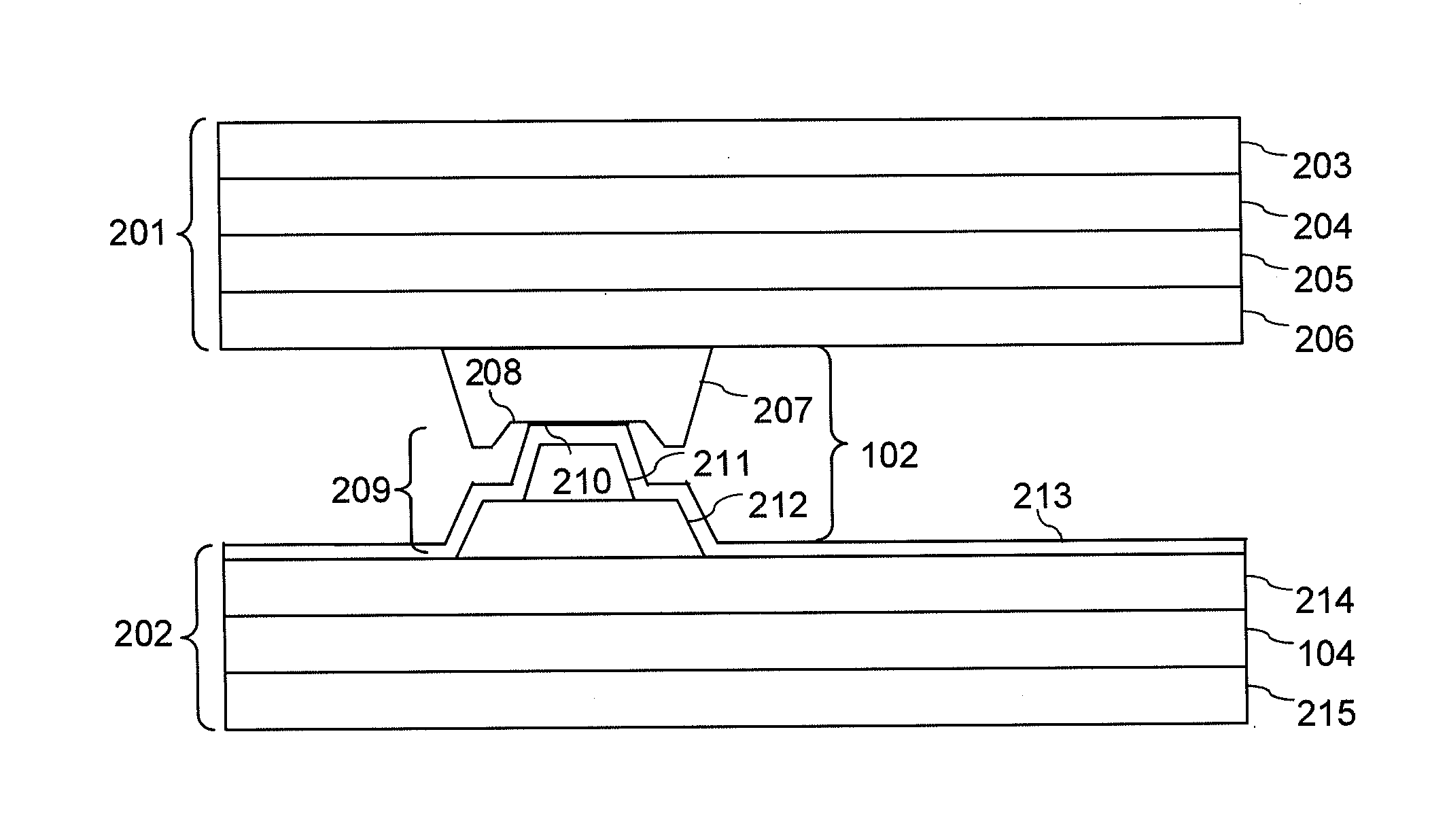
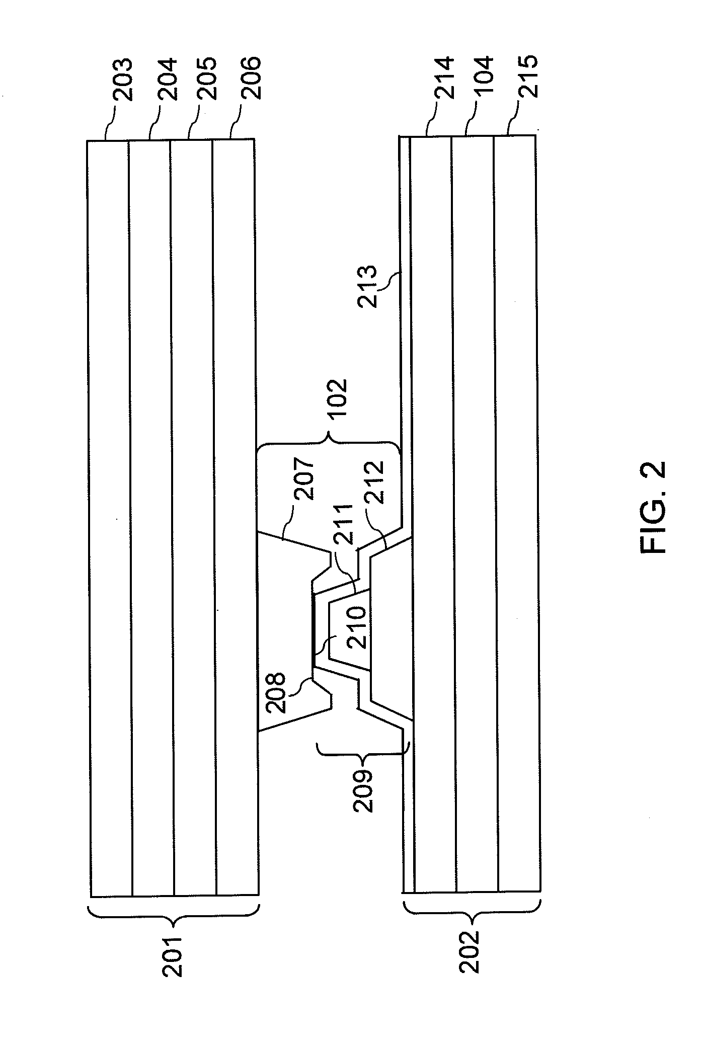
[0031]Referring to FIG. 1, FIG. 1 is a schematic drawing illustrating a position of a spacer 102 in an LCD panel of the present invention. To observe the LCD panel of the present invention in a top view, as shown in FIG. 1, the array substrate 202 of the present invention has a gate line 104, a data line 105, a thin-film transistor 101, a drain line 103, and a pixel electrode 106. The spacer 102 is located at the front of the gate line 104 of the array substrate 202 (to observe the LCD panel of the present invention in a top view). The spacer 102 of the present invention also can be located at the front of the data line 105.

[0032]In the LCD panel of the present invention, the spacer 102 is positioned above the gate line 104 (in a cross-sectional view taken along line A-A′) and / or above the data line 105. Hence, the spacer 102 does not exert a force on the t...


PUM

PropertyMeasurementUnit
shapeaaaaaaaaaa
areaaaaaaaaaaa
transparentaaaaaaaaaa

Abstract

The present invention discloses a liquid crystal display (LCD) panel, which includes an array substrate; a color filter (CF) substrate disposed opposite to the array substrate; and a spacer disposed between the array substrate and the CF substrate. The spacer includes a columnar platform and a recessed platform, and the columnar platform and the recessed platform engage each other. The present invention further discloses a method for manufacturing the LCD panel.

Description

FIELD OF THE INVENTION[0001]The present invention relates to a liquid crystal display (LCD) technology, and especially to an LCD panel and a method for manufacturing the same.BACKGROUND OF THE INVENTION[0002]A conventional LCD panel includes a color filter (CF) substrate, an array substrate, and liquid crystals. The CF substrate includes a first glass substrate, a black matrix (BM) layer, a color-pattern layer, and a transparent electrode (indium tin oxide, ITO) layer. All of the first glass substrate, the BM layer, the color-pattern layer, and the transparent electrode layer are laminated into one body in sequence. The array substrate includes a second glass substrate, a gate line layer, an insulative layer, a semiconductor layer, a metal layer, and a passivation layer. All of the second glass substrate, the gate line layer, the insulative layer, the semiconductor layer, the metal layer, and the passivation layer are laminated into one body in sequence.[0003]The CF substrate and th...

Claims


Application Information

Patent Timeline
Patent Type & Authority Applications(United States)
IPC IPC(8): G02F1/1339H01J9/26
CPCG02F1/13394G02F1/136286G02F1/13398G02F1/1339G02F1/13392
Inventor WU, JO SHANLEE, KUANCHENG
Owner TCL CHINA STAR OPTOELECTRONICS TECH CO LTD
Learn More