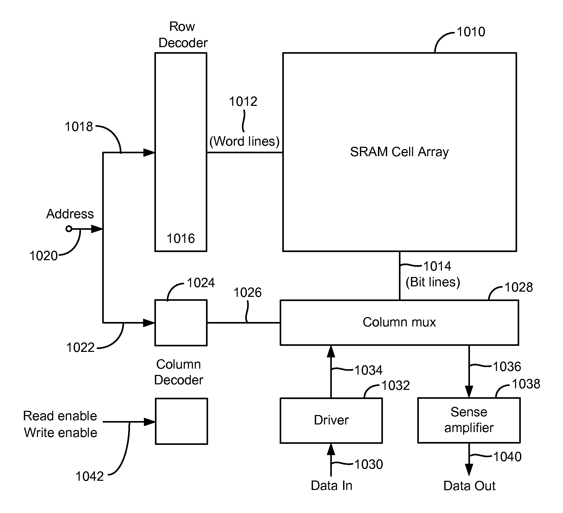
SRAM layouts

a layout and array technology, applied in the field of sram array and cell layout, can solve the problems of not allowing such individual transistor sizing, becoming very difficult to vary the width of the electrode material sharing a particular track,

Active Publication Date: 2014-01-02
SYNOPSYS INC
View PDF1 Cites 37 Cited by
  • Summary
  • Abstract
  • Description
  • Claims
  • Application Information

AI Technical Summary

Benefits of technology

[0012]An opportunity therefore arises to create robust solutions to the problem of SRAM cell optimization at advanced technology nodes, primarily but not exclusively in FinFET environments.

Problems solved by technology

As feature sizes continue to shrink, it has become very difficult to vary the width of the electrode material sharing a particular track.
The difficulty arises in part because of diffraction artifacts caused by sub-wavelength lithography.
Unfortunately, the SRAM layout of FIG. 2 does not permit such individual transistor sizing.

Method used


Image

  • SRAM layouts
  • SRAM layouts
  • SRAM layouts

Examples


Embodiment Construction

[0025]The following description is presented to enable any person skilled in the art to make and use the invention, and is provided in the context of a particular application and its requirements. Various modifications to the disclosed embodiments will be readily apparent to those skilled in the art, and the general principles defined herein may be applied to other embodiments and applications without departing from the spirit and scope of the present invention. Thus, the present invention is not intended to be limited to the embodiments shown, but is to be accorded the widest scope consistent with the principles and features disclosed herein.

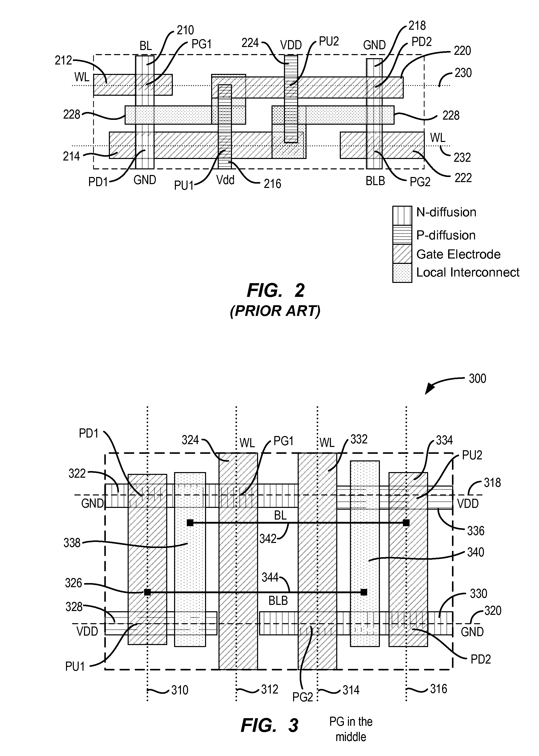
[0026]FIG. 3 is a plan view of an example layout 300 incorporating aspects of the invention, of the 6-transistor SRAM circuit of FIG. 1. It includes four gate electrode tracks 310, 312, 314 and 316 rather than two as in FIG. 2, and two diffusion tracks 318, 320 rather than four as in FIG. 2. In particular, the layout includes an N-channel diffu...


PUM


Abstract

Roughly described, the cell layout in an SRAM array is re-arranged such that the gate electrodes for transistors for which flexibility to use one channel length is desired, are formed along a different track from those for transistors for which flexibility to use a different channel length is desired. Not only does such a re-arrangement permit optimization of device ratios, but also in certain implementations can also reduce, rather than increase, cell area. Specific example layouts are described. The invention also involves layout files, macrocells, lithographic masks and integrated circuit devices incorporating these principles, as well as fabrication methods.

Description

CROSS-REFERENCE TO OTHER APPLICATIONS[0001]This application is a non-provisional of U.S. Provisional Application No. 61 / 690,563, filed 28 Jun. 2012, which is incorporated herein by reference in its entirety.BACKGROUND[0002]1. Field of the Invention[0003]The invention relates to static random access memory (SRAM), and more particularly to SRAM array and cell layouts, layout methods for such memories, and related technologies.[0004]2. Description of Related Art[0005]In most integrated circuit designs, SRAM is a critical component that occupies relatively large area, draws significant power, and determines chip performance. Despite feature size scaling, the minimum channel length in an SRAM cell remains nearly twice as large as that in core logic areas, due to the need to control variability and leakage.[0006]A typical 6-transistor SRAM cell 100 circuit schematic is shown in FIG. 1. It is based on a pair of cross-connected inverters, and includes a first inverter made with a first P-ch...

Claims


Application Information

Patent Timeline
Patent Type & Authority Applications(United States)
IPC IPC(8): G11C11/419H01L21/8238G06F17/50
CPCG11C11/419G06F17/5072H01L21/823828H01L27/0207G11C11/412G06F30/39G06F30/392H10B10/12G06F30/398
Inventor LIN, XI-WEIMOROZ, VICTOR
Owner SYNOPSYS INC
Why Eureka
Try Eureka