Oxide removal from semiconductor surfaces

a technology of semiconductor surfaces and oxides, applied in semiconductor lasers, semiconductor devices, lasers, etc., can solve the problems of oxidation without detrimental effect, pitting surface, limited effectiveness,

Inactive Publication Date: 2014-01-09
UNIV OF LEEDS
View PDF1 Cites 7 Cited by
  • Summary
  • Abstract
  • Description
  • Claims
  • Application Information

AI Technical Summary

Benefits of technology

[0013]Generally, the predetermined temperature or temperature range at or within which the body is held while exposed to the flux of indium atoms is arranged such that the indium atoms react with the desired oxide or oxides on or in the surface of the body, forming at least the more-volatile oxide In2O (one or more other oxides may be formed as well in certain embodiments). The indium oxide is then desorbed from the surface, along with other more-volatile oxides produced in certain embodiments as a result of the reaction between the original oxides and indium atoms. This technique provides the advantage that lower temperatures can be used than with prior art techniques, and / or damage to the surface can be avoided or reduced.
[0017]As with the first aspect, the predetermined temperature or temperature range is arranged such that indium atoms react with the desired oxide or oxides present in or on the oxidised surface of the body of semiconductor material to produce more-volatile compounds which can then be desorbed from the body surface. In this way, the undesired oxide or oxides present on the surface initially can be substantially completely removed, leaving a semiconductor surface suitable for epitaxial overgrowth.
[0038]After using prior art oxide removal techniques, it was typically necessary to grow thicker layers or films (e.g. buffer layers) over the “cleaned” surface before continuing to build up the semiconductor device or other structure, in order to compensate for surface imperfections (i.e. defects or damage) caused by the prior art oxide removal techniques. However, in certain embodiments of the invention, the use of indium flux to remove oxides enables those oxides to be removed in a manner which avoids or reduces damage or degradation to the surface being cleaned, and hence much thinner epitaxial layers or films (e.g. buffer layers) may be required.
[0050]Similarly, this third predetermined range may be the same or different from the first and second predetermined ranges mentioned above, or in alternative embodiments may be different. Similarly, the third predetermined temperature may be the same as one of the first and second predetermined temperatures, or may be different. Generally, the third predetermined range or third predetermined temperature are arranged in combination with the particular materials involved to assist in the reaction of the As with products of the previous reaction between the indium flux and the semiconductor surface, including any oxides, to aid cleaning of the semiconductor surface.
[0067]The above-mentioned range of indium atom concentration in the patterned surface is a signature of the fact that the patterned surface has been processed by a method in accordance with another aspect of this invention (i.e. by exposing the surface to a flux of indium atoms at a suitable temperature and within a suitable temperature range). Furthermore, the small thickness of the epitaxial layer or film grown over the patterned surface is indicative of the fact that the indium technique of embodiments of the present invention has been used to clean oxides from the patterned surface. The lack of surface damage resulting from use of the method embodying the invention enables such a thin layer or film to be utilised.

Problems solved by technology

A general problem is how to remove such oxides without detrimentally affecting the semiconductor body surface.
Such cleaning requires temperatures in excess of ˜580° C. and an As overpressure, but can have limited effectiveness.
Thermal cleaning of the GaAs surface, therefore, tends to result in a pitted surface owing to GaAs removal from the substrate.
However, this method is known to lead to Fermi-level surface pinning and possible degradation of the surface if the hydrogen dose is not precisely controlled.
In addition, surface contamination could be introduced during the hydrogen-assisted cleaning process, if extreme care is not taken.
However, the technique is very sensitive to the precise amount of oxide on the surface.

Method used


Image

  • Oxide removal from semiconductor surfaces
  • Oxide removal from semiconductor surfaces
  • Oxide removal from semiconductor surfaces

Examples


Embodiment Construction

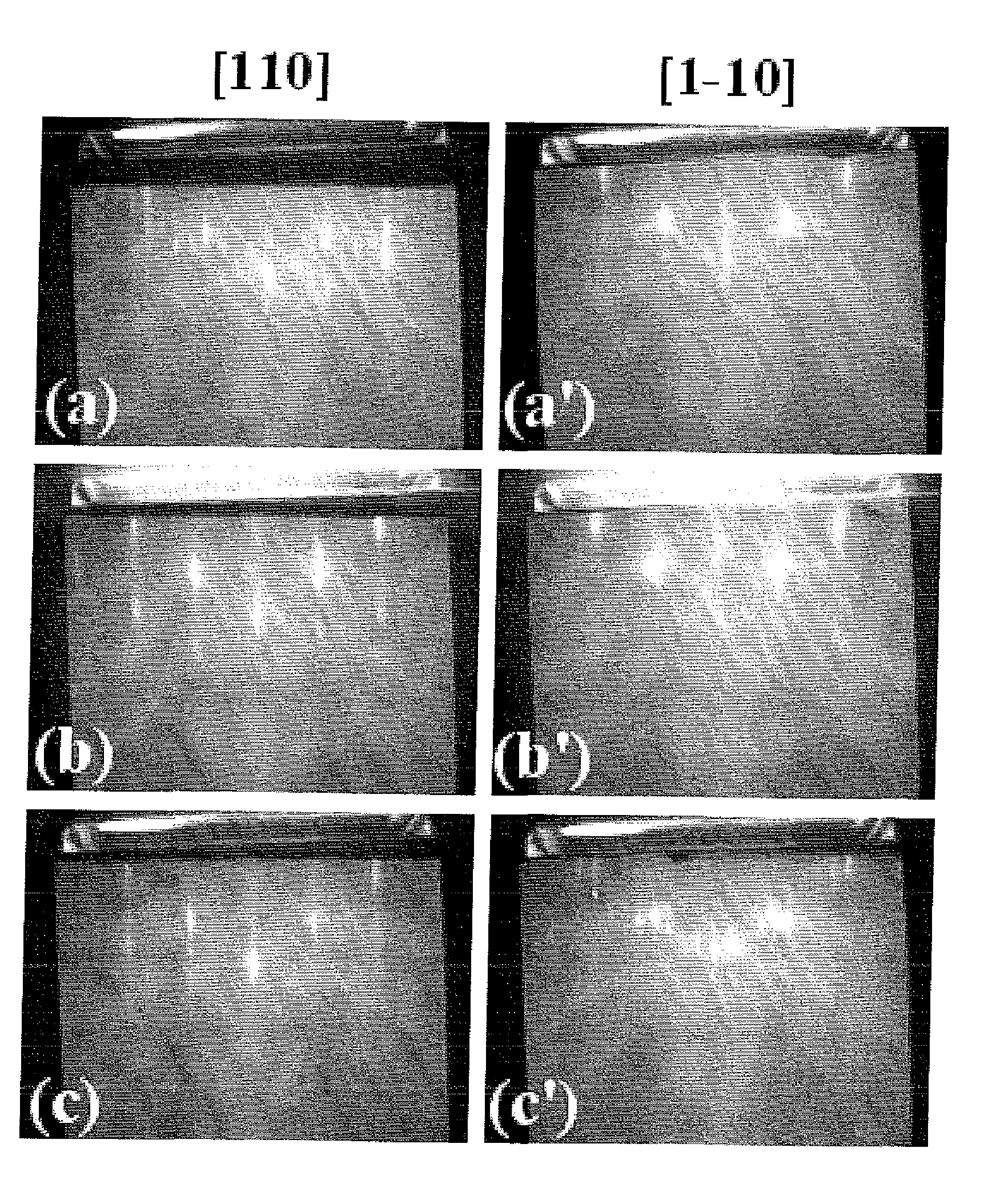
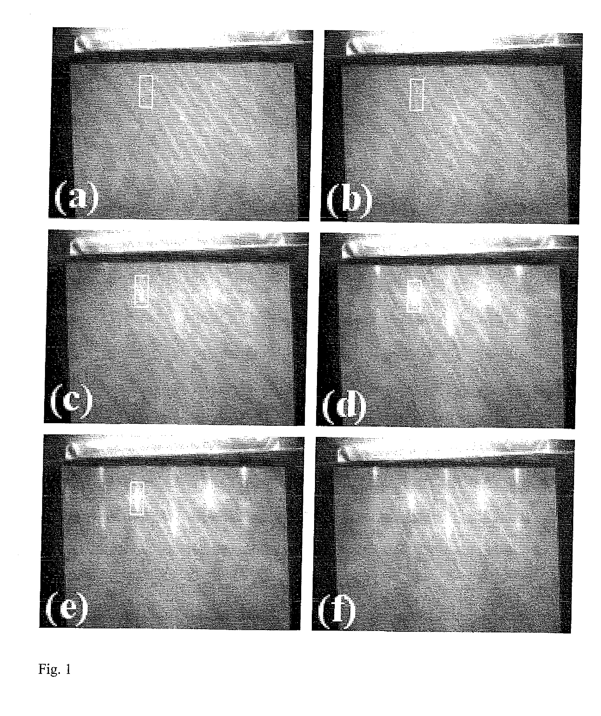
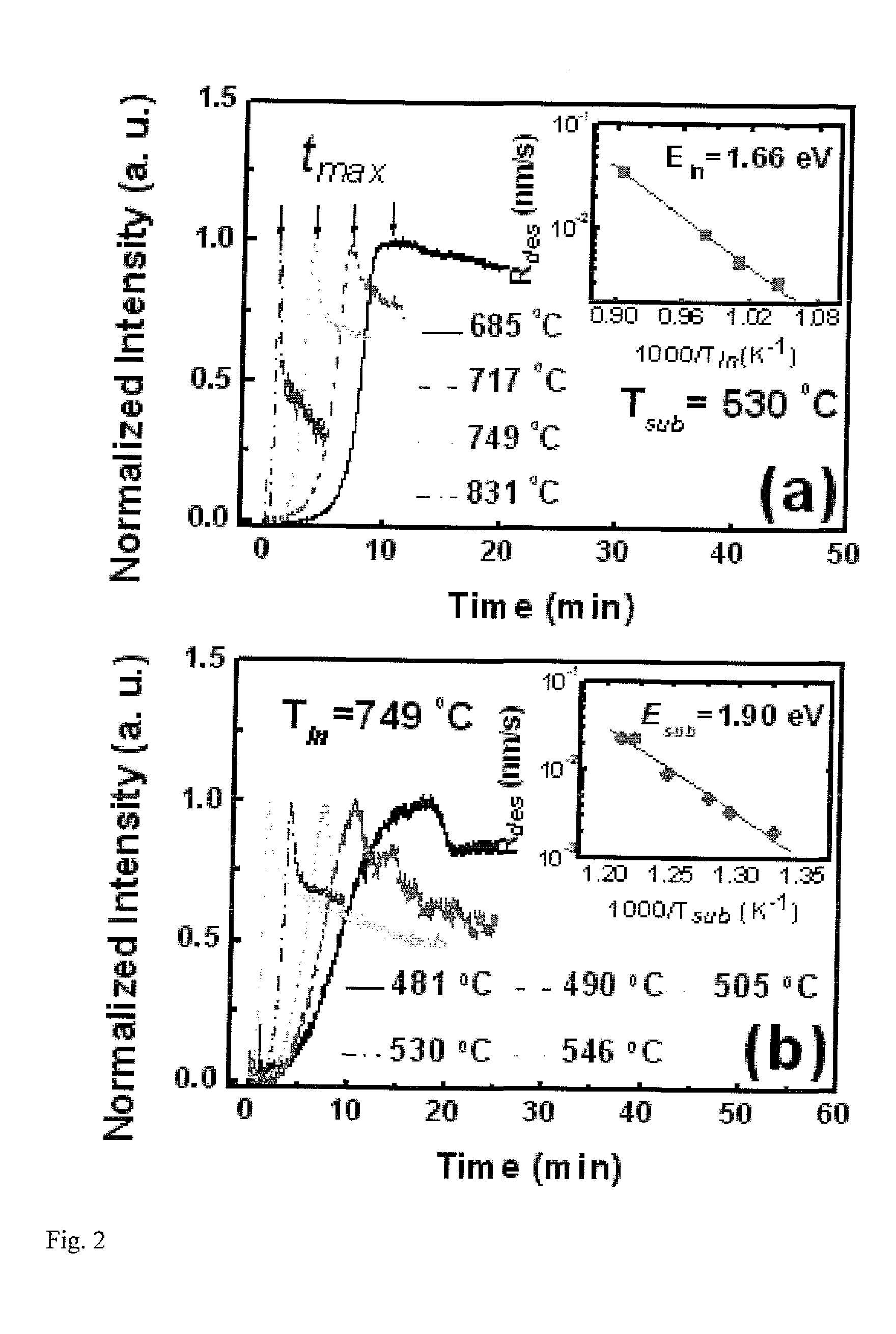
[0081]Certain embodiments provide Indium-assisted desorption of native GaAs surface oxides. In the following description, indium-assisted desorption of native GaAs surface oxides at substrate temperatures of 480-550° C. is described. The oxides are removed through production of volatile gallium and indium suboxides, Ga2O and In2O. Compared to a gallium-assisted desorption process, excess indium is easily removed at low temperature, leading to a clean, smooth surface. The feasibility of using indium-assisted desorption for the regrowth of high quality quantum dot structures is shown.

[0082]To overcome problems associated with prior art techniques, indium is used in certain embodiments of the invention as an alternative element which can react with Ga2O3 to produce volatile products, and which can also itself be readily evaporated at lower temperature from the underlying GaAs substrate. Compared with gallium, indium has a relatively large atomic size as well as a high vapour pressure. ...


PUM

PropertyMeasurementUnit
thicknessaaaaaaaaaa
temperatureaaaaaaaaaa

Abstract

A method of removing at least one oxide from a surface of a body of semiconductor material is disclosed, the method comprising: arranging the body in a vacuum chamber; and maintaining a temperature of the body in the vacuum chamber within a predetermined range, or substantially at a predetermined value, while exposing said surface to a flux of indium atoms. Corresponding methods of processing an oxidised surface of a body of semiconductor material to prepare the surface for epitaxial growth of at least one epitaxial layer or film over said surface, and methods of manufacturing a semiconductor device are also disclosed.

Description

FIELD OF THE INVENTION[0001]The present invention generally relates to the use of indium to remove oxide from a semiconductor surface, and to semiconductor devices produced using such techniques. Particular embodiments relate to the use of a flux of indium atoms to remove oxide from a semiconductor surface to prepare that surface for overgrowth of at least one epitaxial layer or film.BACKGROUND TO THE INVENTION[0002]A wide variety of techniques for the manufacture of semiconductor devices and semiconductor structures are known. These include, for example, techniques in which a layer, film, or some other body of material is formed over a body of semiconductor material. For numerous reasons it may be desirable to remove oxides from the surface of the body of semiconductor material before the body of material is formed over it. A general problem is how to remove such oxides without detrimentally affecting the semiconductor body surface. More specific problems will be appreciated from t...

Claims


Application Information

Patent Timeline
Patent Type & Authority Applications(United States)
IPC IPC(8): H01L21/02
CPCH01L21/02661B82Y20/00H01L21/02H01L21/02395H01L21/0243H01L21/02463H01L21/02546H01L21/0259H01L21/0262H01L21/02631H01L21/20H01L21/306H01S5/1231H01S5/3412H01S2304/02
Inventor LI, LIANHEDAVIES, ALEXANDERLINFIELD, EDMUND
Owner UNIV OF LEEDS
Why Eureka
Try Eureka