Lamb wave device and manufacturing method thereof

a technology of a lamb wave and a manufacturing method, which is applied in the direction of piezoelectric/electrostrictive transducers, generators/motors, transducer types, etc., can solve the problems of reducing the degree of freedom in selecting materials. , to achieve the effect of limiting the piezoelectric characteristics and lowering the degree of freedom in selecting materials

Active Publication Date: 2014-01-09
TAIYO YUDEN KK
View PDF8 Cites 39 Cited by
  • Summary
  • Abstract
  • Description
  • Claims
  • Application Information

AI Technical Summary

Benefits of technology

[0011]However, the configuration described in Patent Document 1 has a problem of requiring a thickness control for not only the piezoelectric substrate, but also the adjustment film. The technique described in Patent Document 2 lowers a degree of freedom in selecting the material, and possibly puts a limitation on the piezoelectric characteristics.

Problems solved by technology

However, the configuration described in Patent Document 1 has a problem of requiring a thickness control for not only the piezoelectric substrate, but also the adjustment film.
The technique described in Patent Document 2 lowers a degree of freedom in selecting the material, and possibly puts a limitation on the piezoelectric characteristics.

Method used


Image

  • Lamb wave device and manufacturing method thereof
  • Lamb wave device and manufacturing method thereof
  • Lamb wave device and manufacturing method thereof

Examples


embodiment 1

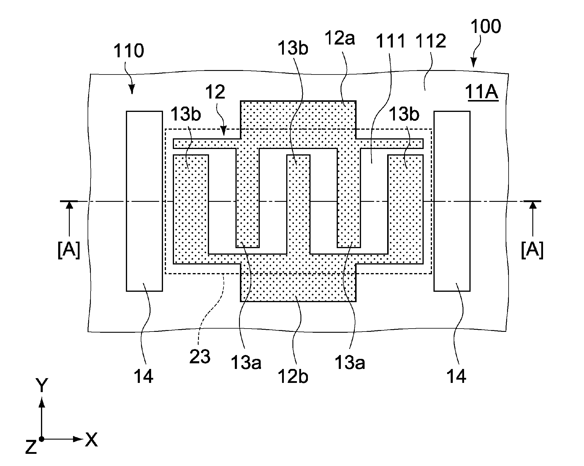
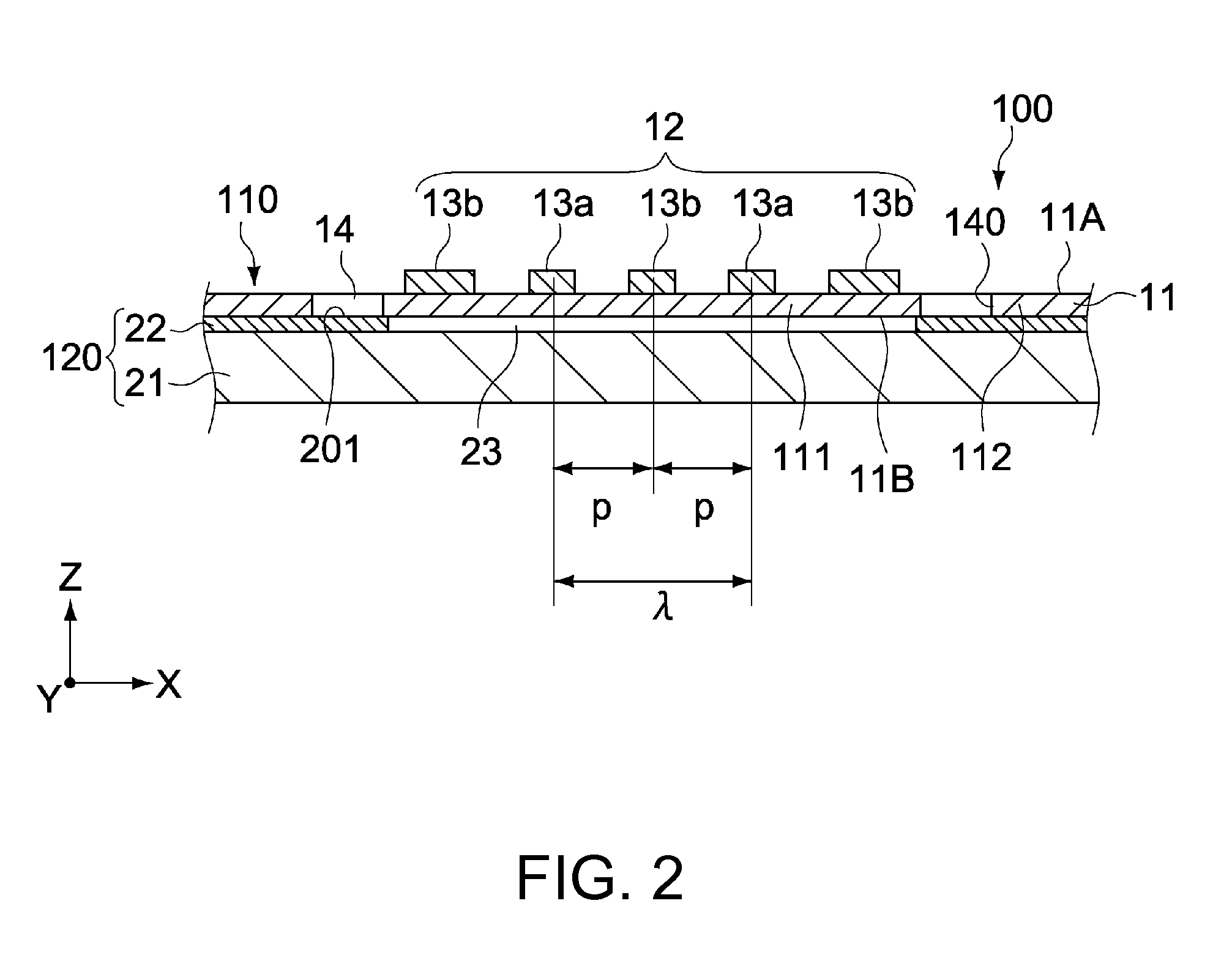
[0055]FIGS. 1 and 2 are schematic diagrams showing a configuration of a Lamb wave device according to Embodiment 1 of the present invention. FIG. 1 is a plan view, and FIG. 2 is a cross-sectional view along the line A-A in FIG. 1. In each figure, respective axis directions of X, Y, and Z represent three axis directions that are orthogonal to each other, and the Z axis direction corresponds to the thickness direction (height direction) of the Lamb wave device.

[0056](Overall Configuration)

[0057]A Lamb wave device 100 of this embodiment has a piezoelectric function member 110 and a supporting member 120. The Lamb wave device 100 in this embodiment is configured as a Lamb wave resonator that is used in a transmitting / receiving filter of portable devices.

[0058]The piezoelectric function member 110 has a piezoelectric substrate 11 and IDT electrodes 12. The supporting member 120 has a supporting substrate 21 and a bonding layer 22. The supporting member 120 supports the piezoelectric subs...

embodiment 2

[0113]FIGS. 6 and 7 are schematic diagrams showing a configuration of a Lamb wave device of Embodiment 1 of the present invention. FIG. 6 is a plan view showing two adjacent device regions at wafer level, and FIG. 7 is a cross-sectional view along the B-B line in FIG. 6. FIG. 8 is a plan view of the piezoelectric substrate as a wafer.

[0114]In each figure, respective axis directions of X, Y, and Z represent three axis directions that orthogonal to each other, and the Z axis direction corresponds to the thickness direction (height direction) of the Lamb wave device. Below, differences from Embodiment 1 will be mainly explained. Configurations similar to those of Embodiment 1 are given similar reference characters, and descriptions thereof are omitted or simplified.

[0115]A Lamb wave device 200 of this embodiment has a piezoelectric function member 210 and a supporting member 220. The piezoelectric function member 210 has a piezoelectric substrate 11W (11), IDT electrodes 12, and a cuto...

embodiment 3

[0122]FIGS. 10 to 12 are schematic diagrams showing a configuration of a Lamb wave device of Embodiment 3 of the present invention. FIG. 10 is a plan view showing two adjacent device regions at wafer level, and FIG. 11 is a cross-sectional view along the line C-C in FIG. 10. FIG. 12 is a cross-sectional view showing a principal portion of the Lamb wave device.

[0123]In each figure, respective axis directions of X, Y, and Z represent three axis directions that orthogonal to each other, and the Z axis direction corresponds to the thickness direction (height direction) of the Lamb wave device. Below, differences from Embodiment 1 will be mainly explained. Configurations similar to those of the embodiments above are given similar reference characters, and descriptions thereof are omitted or simplified.

[0124]A Lamb wave device 300 of this embodiment has a piezoelectric function member 310 and a supporting member 320. The piezoelectric function member 310 has a piezoelectric substrate 11W ...


PUM

PropertyMeasurementUnit
opening widthaaaaaaaaaa
frequencyaaaaaaaaaa
frequencyaaaaaaaaaa

Abstract

A Lamb wave device according to an embodiment of the present invention includes a piezoelectric function member and a supporting member. The piezoelectric function member has a piezoelectric substrate, IDT electrodes, and a cutout portion. The IDT electrodes are disposed on the upper surface of the piezoelectric substrate. The cutout portion is formed in the piezoelectric substrate, and includes a step face provided between the upper surface and the lower surface of the piezoelectric substrate. The supporting member has a supporting surface and a cavity. The supporting surface is bonded to the lower surface of the piezoelectric substrate, and is exposed in the cutout portion toward the upper surface of the piezoelectric substrate. The cavity is formed adjacent to the supporting surface, and faces the IDT electrodes through the piezoelectric substrate.

Description

[0001]This application claims the benefit of Japanese Patent Application No. 2012-150295, filed in Japan on Jul. 4, 2012, which is hereby incorporated by reference in its entirety.BACKGROUND OF THE INVENTION[0002]1. Field of the Invention[0003]The present invention relates to a Lamb wave device that uses Lamb waves, and to a method of manufacturing same.[0004]2. Description of Related Art[0005]Surface acoustic wave (SAW) filters and film bulk acoustic resonators (FBAR) are used in mobile phones to transmit and receive radio waves. SAW filters are mainly used for a frequency range of 3 GHz or lower, for example, and FBARs are mainly used for a frequency range of 1.6 GHz or higher, for example. Because next generation mobile phones use radio waves in the 3.5 GHz band, filter devices used for such next generation mobile phones are required to be able to handle a higher frequency than conventional filters (2 GHz band). In order to meet such demands, Lamb wave devices have been developed...

Claims


Application Information

Patent Timeline
Patent Type & Authority Applications(United States)
IPC IPC(8): H01L41/053H01L41/29
CPCH01L41/053H01L41/29H03H9/02228H03H9/059Y10T29/42H10N30/88H03H9/02015H03H9/02559H10N30/06
Inventor TAKAHASHI, TOMOYUKIIRIEDA, TAISEINAKAMURA, KENTARO
Owner TAIYO YUDEN KK
Why Eureka
Try Eureka