Capacitor and method of manufacturing the same

a technology of capacitors and capacitors, applied in the field of capacitors, can solve the problems of crosstalk noise occurring among wirings, fluctuation of electric potential, and likely frequency-related crosstalk noise, and achieve the effect of reducing costs

Active Publication Date: 2011-01-20
SHINKO ELECTRIC IND CO LTD
View PDF8 Cites 17 Cited by
  • Summary
  • Abstract
  • Description
  • Claims
  • Application Information

AI Technical Summary

Benefits of technology

[0015]An object of the present invention is to provide a capacitor which is capable of increasing a capacitance thereof by allowing the capacitance to be easily changed without being restricted by any design, and which can be easily mounted inside a board, and a method of manufacturing the capacitor.
[0016]Another object of the present invention is to provide a method of manufacturing a capacitor, which contributes to a reduction in time required for the manufacturing and a reduction in cost.
[0019]In this arrangement, one of the electrodes and the plurality of filamentous conductors connected thereto are not electrically connected to the other one of the electrodes and the plurality of filamentous conductors connected thereto, and thus the structure in which capacitive coupling is realized through only the dielectric (dielectric substrate) is achieved. This configuration allows the capacitor capacitance to be easily changed by varying and designing, as necessary, the sizes of the respective electrodes disposed on the dielectric substrate and the relative positions therebetween, thereby making it possible to obtain a required large capacitance without being restricted by any design as encountered in the prior art.
[0020]Further, the capacitor has a planar shape, and the board used as the dielectric has a large number of filamentous conductors formed therein in such a way as to penetrate through the board. Accordingly, the two surfaces of the dielectric substrate can be easily connected to each other through the filamentous conductors. Therefore, when the capacitor is buried into a wiring board (package), no such inconvenience as encountered in the prior art occurs in that the degree of freedom in designing other wiring patterns on the conductor layers in the board is decreased. Thus, the capacitor can be easily included in a board.
[0022]The method of manufacturing a capacitor according to this aspect provides the following advantages, in addition to the effects attained by the capacitor according to the above-described aspect. Namely, there is no requirement for a process to stack an insulating layer (dielectric layer) and a conductor layer (electrode) one above the other as has been carried out in the prior art, and therefore, a shorter term for the manufacturing and a lower cost can be achieved.

Problems solved by technology

Accordingly, there may arise problems such as a crosstalk noise occurring among wirings and a fluctuation in the electric potential of a power-supply line or the like.
Especially, in a package on which a chip such as an MPU (microprocessor unit) requiring a high-speed switching operation is mounted, a crosstalk noise is likely to occur in accordance with an increase in frequency.
In addition, some switching noise occurs when a switching element is turned on and off at a high speed, resulting in the likelihood of fluctuation in the electric potential of a power-supply line or the like.
In the configuration in which a component (chip capacitor) is surface-mounted on a board, however, the mounting of the component makes it difficult to reduce the thickness of the board.
Further, this configuration poses a problem as follows.
Moreover, when a semiconductor element requiring a high-speed switching operation is mounted, a large number of chip capacitors need to be provided to achieve the desired decoupling effect.
Accordingly, there also arises a problem in that a process required for mounting the chip capacitors becomes longer.
However, the former configuration has a problem in that it is difficult to obtain a large capacitance due to design restrictions as follows.
Accordingly, the area occupied by the electrodes is increased, and thus there has been an inconvenience that the degree of freedom in design of other wiring patterns on the conductor layers is reduced.
As a result, there arises a problem in that it is difficult to incorporate a capacitance structure having a desirably large capacitance into the wiring board.
Accordingly, the term required for manufacturing becomes longer, resulting in an increase in the manufacturing cost.

Method used


Image

  • Capacitor and method of manufacturing the same
  • Capacitor and method of manufacturing the same
  • Capacitor and method of manufacturing the same

Examples


first embodiment

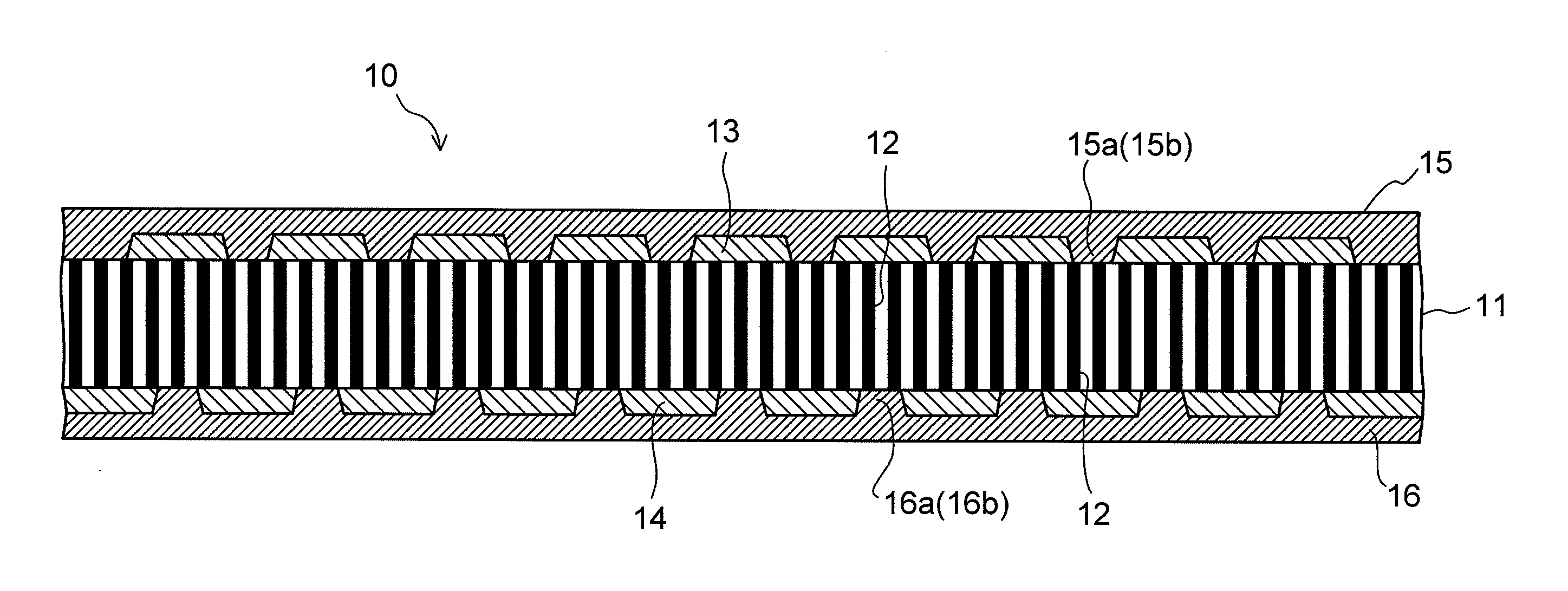
[0032]FIG. 1 is a cross-sectional view of a structure of a capacitor according to the present invention. Although capable of being used as a single product by itself, a capacitor 10 of the present embodiment is basically intended to be used as being buried in a wiring board (package) on which an electronic component (chip) such as a semiconductor element is to be mounted.

[0033]The capacitor 10 of the present embodiment has a basic structure including: a dielectric substrate 11 having a desired thickness; and filamentous conductors 12 each having a small diameter, penetrating through the dielectric substrate 11 in a thickness direction thereof, and being disposed densely at predetermined intervals. Specifically, the filamentous conductors 12 are formed in such a way as to expose ends thereof from both surfaces of the dielectric substrate 11, respectively. For the dielectric substrate 11, it is desirable to use a material having a highest possible permittivity, and an inorganic materi...

second embodiment

[0060]FIG. 5 is a cross-sectional view showing a structure of a capacitor according to the present invention.

[0061]A capacitor 20 (FIG. 5) of the present embodiment is different from the capacitor 10 (FIG. 1) of the first embodiment in terms of arrangements with respect to the following points: conductor layers 25 and 26 formed respectively on both surfaces of the capacitor 20 are each divided into two conductor layer regions in the illustrated example; insulating layers 23 and 24 respectively formed on the surfaces of the dielectric substrate 11 are exposed at portions where the conductor layers 25 and 26 are each divided into the two conductor layer regions; and an electrode 25b out of multiple electrodes 25a and 25b concurrently connected to the conductor layer 25 and an electrode 26b out of multiple electrodes 26a and 26b concurrently connected to the conductor layer 26 are disposed so as to face each other with the dielectric substrate 11 in between, and are electrically connec...

third embodiment

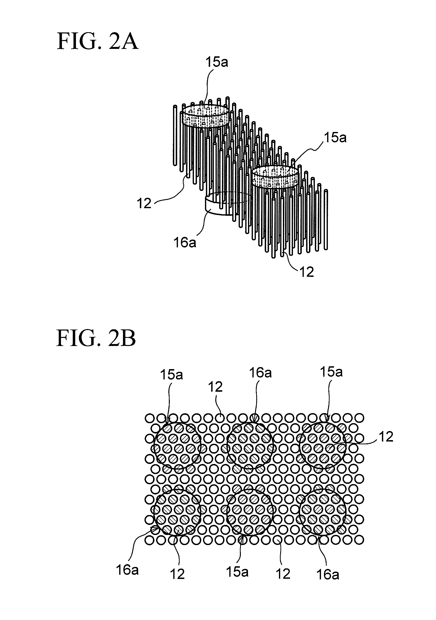
[0067]FIG. 6 is a perspective view schematically showing a configuration of a main portion (the filamentous conductors 12 and electrodes 35 and 36 connected thereto) of a capacitor 30 according to the present invention. FIGS. 7A and 7B show a structure of the capacitor 30, and are views showing cross-sectional structures taken along the line A-A′ and the line B-B′ in FIG. 6, respectively.

[0068]The capacitor 30 (FIGS. 7A and 7B) of the present embodiment is different from the capacitor 10 (FIG. 1) of the first embodiment in terms of arrangements with respect to the following points: the electrodes 35 and 36 to be disposed respectively on both surfaces of the dielectric substrate 11 (having the filamentous conductors 12 formed in such a way as to penetrate through the dielectric substrate 11 in a thickness direction thereof) are formed to have a comb-pattern shape; the electrodes 35 and 36 respectively include narrow line portions (comb-tooth portions) 35a and 36a, which extend parall...


PUM

PropertyMeasurementUnit
diameteraaaaaaaaaa
sizeaaaaaaaaaa
sizeaaaaaaaaaa

Abstract

A capacitor includes a dielectric substrate and a large number of filamentous conductors formed to penetrate through the dielectric substrate in a thickness direction thereof. An electrode is connected to only respective one ends of a plurality of filamentous conductors constituting one of groups each composed of a plurality of filamentous conductors. The electrode is disposed in at least one position on each of both surfaces of the dielectric substrate, or in at least two positions on one of the surfaces. Further, an insulating layer is formed on each of both surfaces of the dielectric substrate so as to cover regions between the electrodes, and a conductor layer is formed on the corresponding insulating layer integrally with a desired number of electrodes.

Description

CROSS-REFERENCE TO RELATED APPLICATIONS[0001]This application is based on and claims priority of Japanese Patent Application No. 2009-165280 filed on Jul. 14, 2009, the entire contents of which are incorporated herein by reference.BACKGROUND OF THE INVENTION[0002](a) Field of the Invention[0003]The present invention relates to a capacitor and a method of manufacturing the same. Particularly, it relates to a capacitor which is adapted to be buried into a wiring board on which an electronic component (chip) such as a semiconductor element is to be mounted, and to a method of manufacturing the capacitor.[0004]Since a wiring board having such a capacitor incorporated therein plays a role in mounting of a semiconductor element or the like, the wiring board is also referred to as a “semiconductor package” or simply a “package” for convenience in the description below.[0005](b) Description of the Related Art[0006]With the demand for further miniaturization and high-density of wirings in a ...

Claims


Application Information

Patent Timeline
Patent Type & Authority Applications(United States)
IPC IPC(8): H01G4/06H05K3/30
CPCH05K2201/097H05K1/162H05K2201/09945Y10T29/4913H01G4/012H05K2201/09609H01G4/232H05K2201/09263H05K1/0287H05K1/0306H01G4/302Y10T29/435H05K2201/09563
Inventor HORIUCHI, MICHIOTOKUTAKE, YASUEMATSUDA, YUICHISHIMIZU, YUKIOYAMASAKI, TOMOOSAKAGUCHI, YUTA
Owner SHINKO ELECTRIC IND CO LTD
Why Eureka
Try Eureka