

CMOS Switching Circuitry of a Transmitter Module
a transmitter module and circuitry technology, applied in electronic switching, amplifiers with semiconductor devices/discharge tubes, pulse techniques, etc., can solve problems such as difficult bulk cmos implementation of switches, distortion and breakdown of transistors, and breakdown of mos oxides or drain and source diodes
- Summary
- Abstract
- Description
- Claims
- Application Information
AI Technical Summary
Benefits of technology
Problems solved by technology
Method used
Image

Examples
Embodiment Construction
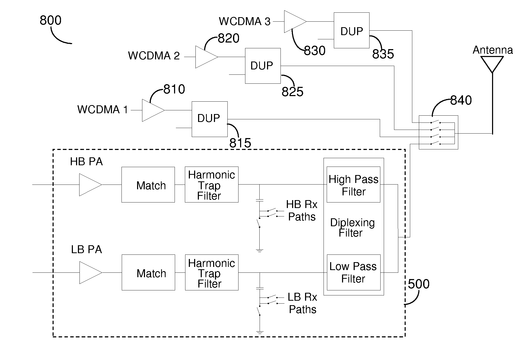
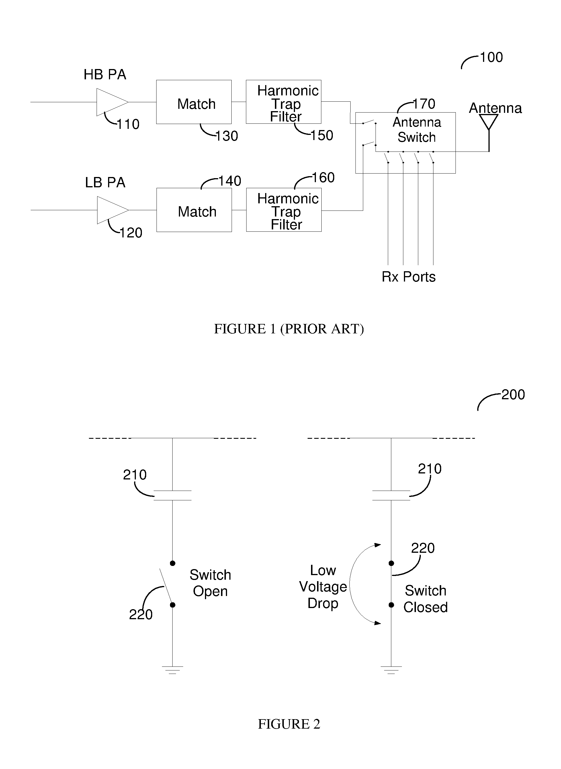
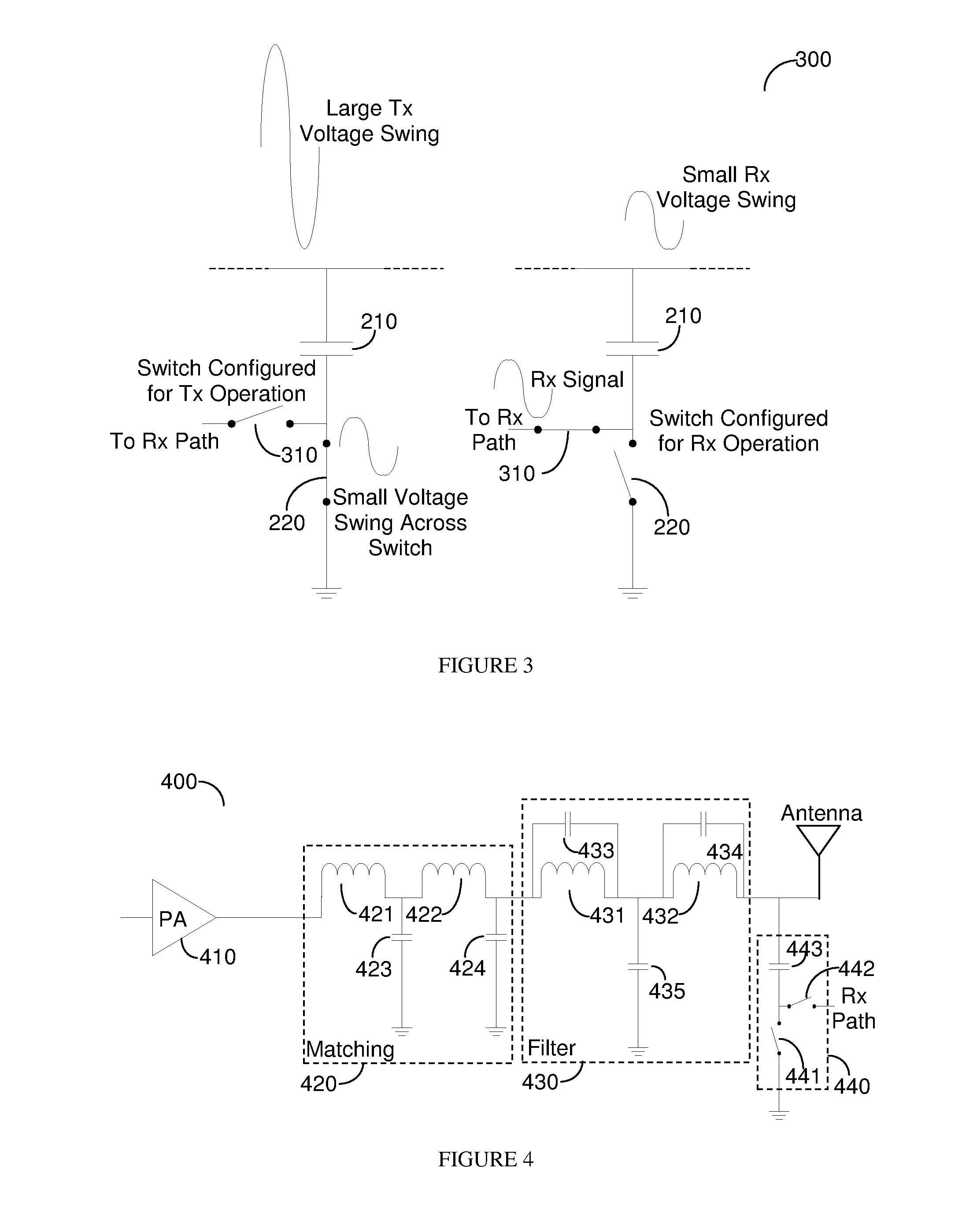
[0016]Transmit modules typically constitute passive matching circuitry, harmonic trap filters and an antenna switch to provide isolation between the transmit bands as well as between transmit and receive functions. In complementary metal-oxide semiconductor (CMOS) processes the switch function is difficult to implement as a large voltage swing may result in breakdown of the MOS oxide, drain diode, source diode as well as substrate diodes. Therefore a switching function is provided at a node that has low impedance during transmit that limits the voltage swing that the MOS switches experience. The approach is particularly useful, but not limited to, half duplex transmissions such as those used in global system for mobile (GSM) communication, enhanced data for GSM Evolution (EDGE), and time division synchronous code division multiple access (TDSCDMA).
[0017]The challenge is therefore to avoid having a high voltage swing on the MOS switch, also referred to herein as a switch. FIG. 2 depi...
PUM
 Abstract
Description
Claims
Application Information