Display Device and Method for Manufacturing Display Device

a display device and display technology, applied in the field of display devices, can solve the problems of large deflection of substrates, difficulty in reducing the total thickness of display devices, and reducing yield, so as to reduce the thickness of display devices having high display quality, reduce the thickness of display devices, and reduce the effect of mass productivity

Active Publication Date: 2014-01-16
SEMICON ENERGY LAB CO LTD
View PDF3 Cites 149 Cited by
  • Summary
  • Abstract
  • Description
  • Claims
  • Application Information

AI Technical Summary

Benefits of technology

[0037]According to the present invention, the thickness of a display device including a touch sensor can be reduced. Alternatively, the thickness of a display device having high display quality can be reduced. Alternatively, a display device can be manufactured with high mass productivity. Alternatively, a display device having high reliability can be provided.

Problems solved by technology

In the case of a display device in which a touch sensor and a display portion are stacked, it has been difficult to reduce its total thickness sufficiently.
Although it is possible to reduce the thickness of the display device by, for example, forming a touch sensor and a display element over respective relatively thick substrates at the time of manufacturing the touch sensor and the display portion and then by polishing the back sides of the substrates, the polishing step after manufacturing the elements causes a decrease in yield.
In the case of forming the elements directly over thin substrates, the deflection of the substrates is large, and it is difficult to transport the substrates.
In addition, there arise problems such as breakage of the substrates in transporting or processing the substrates.
In the case of using a thin substrate as that substrate, there have been problems of difficulty in overlapping the color filter and the display element with high alignment accuracy due to the aforementioned deflection of the substrate or the like, and difficulty in achieving both a high display quality and a small thickness of the display device.

Method used


Image

  • Display Device and Method for Manufacturing Display Device
  • Display Device and Method for Manufacturing Display Device
  • Display Device and Method for Manufacturing Display Device

Examples


embodiment 1

[0050]In this embodiment, a configuration example of a display device in one embodiment of the present invention and an example of a manufacturing method thereof will be described with reference to drawings.

example 1

[Manufacturing Method Example 1]

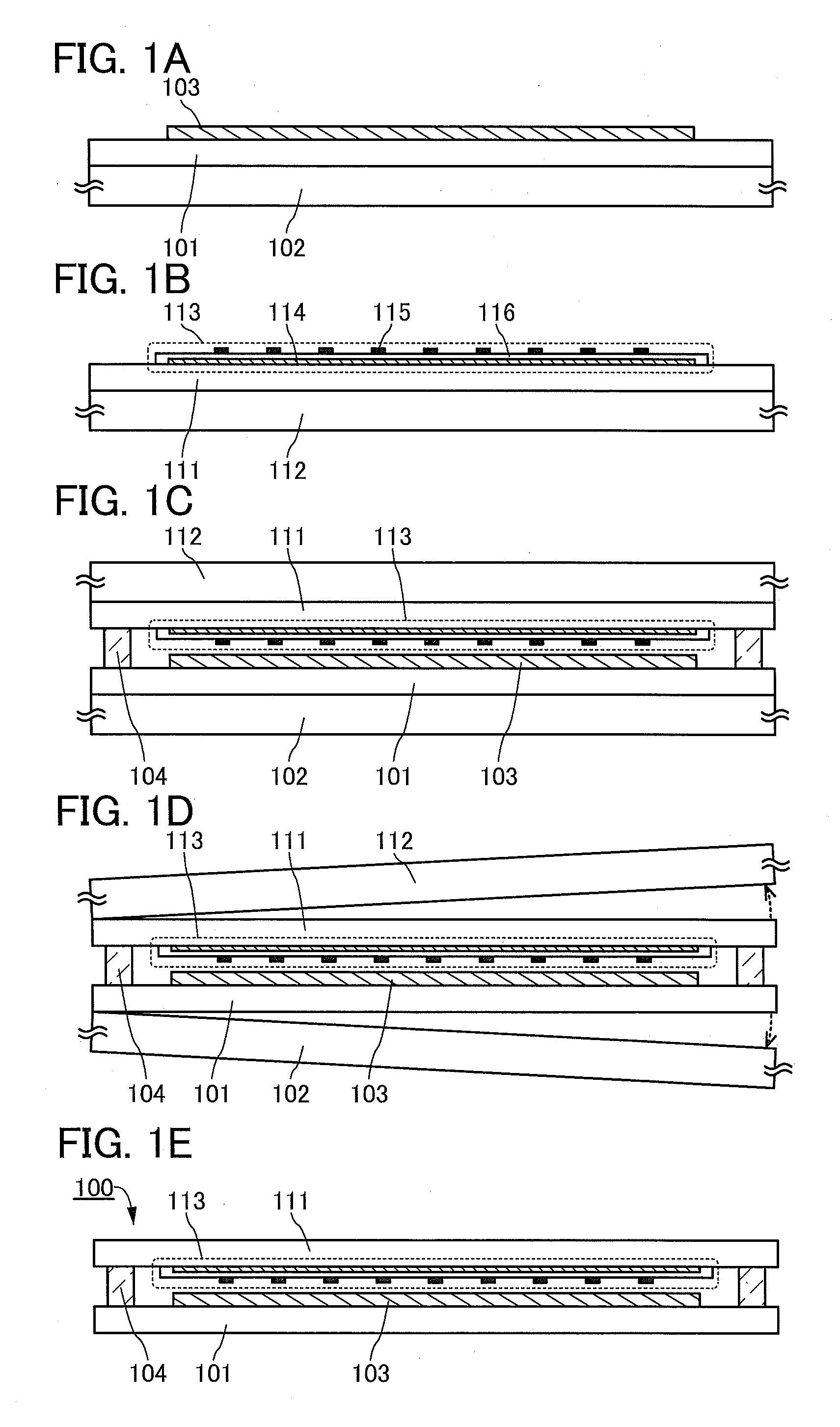
[0051]First, a stacked substrate in which a first substrate 101 is stacked over a first support substrate 102 is prepared.

[0052]As the first substrate 101, a substrate having an insulating surface and having a thickness of 10 μm to 200 μm is used. As a material of the first substrate 101, a glass material, an organic resin material, a conductive material containing a metal or an alloy, or the like can be used.

[0053]It is preferable to use a glass material for the first substrate 101. With the glass material, a large-sized substrate having an extremely flat surface and a uniform thickness can be manufactured with relative ease. Such a glass substrate can be manufactured using a float method, an overflow method, or the like.

[0054]In the case where the first substrate 101 is on a display surface side, a light-transmitting substrate is used. On the other hand, in the case where the first substrate 101 is on a side opposite to the display surface, a non-li...

example 2

[Manufacturing Method Example 2]

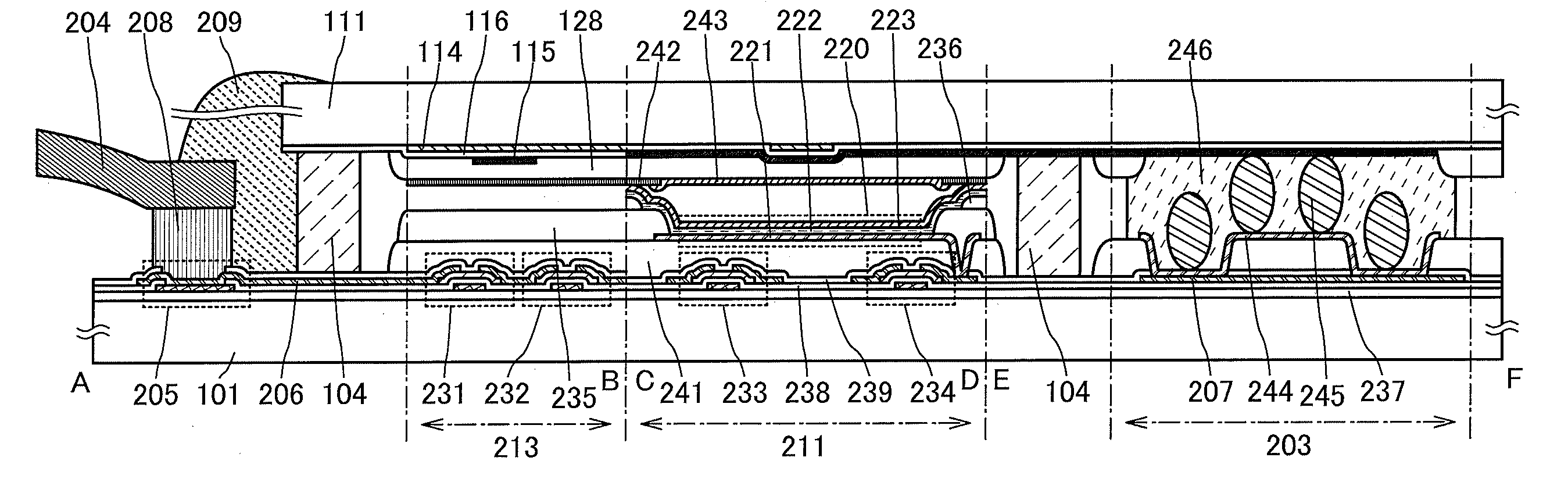
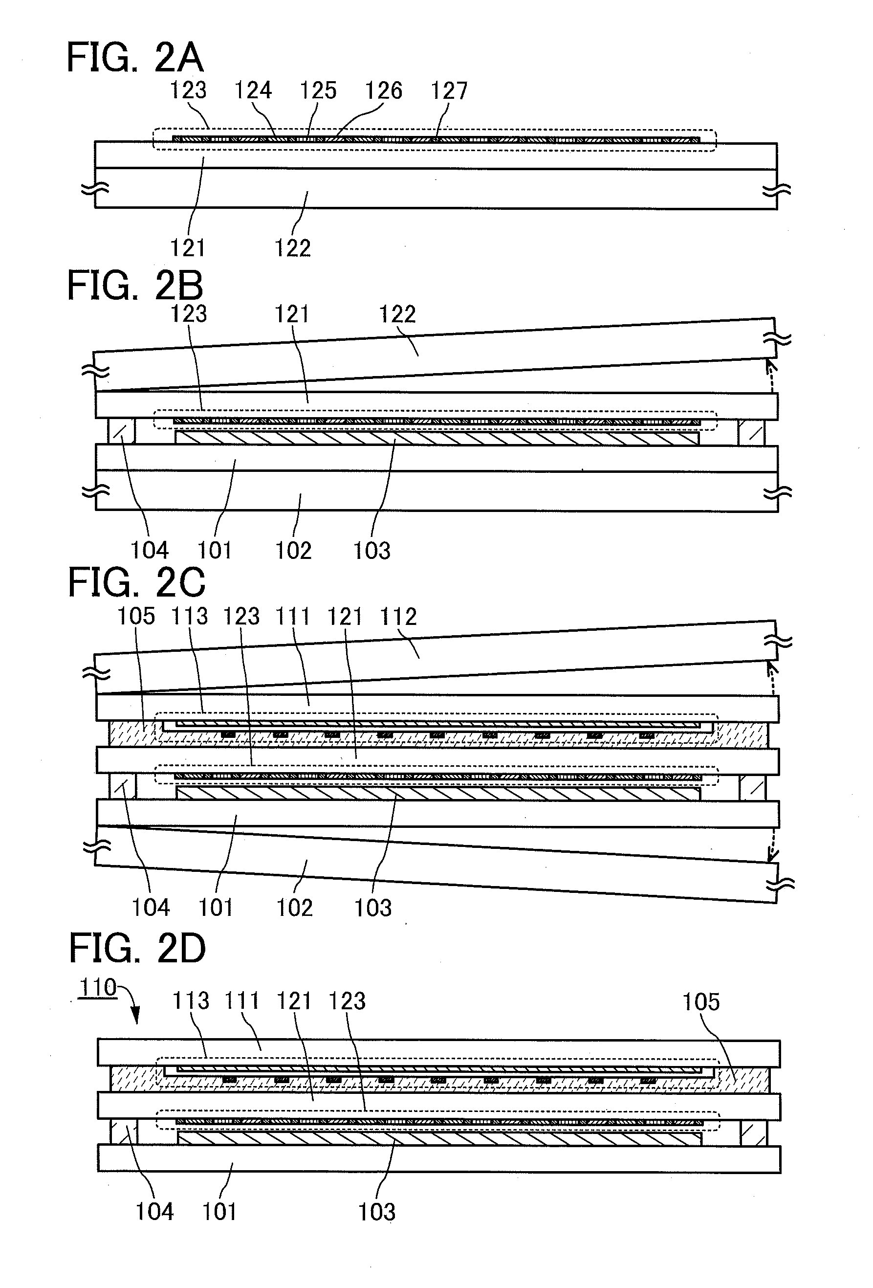
[0088]An example of a method for manufacturing a display device different from that in Manufacturing Method Example 1 will be described below. Specifically, a display device including color filters will be described. Note that description of the portions already described in Manufacturing Method Example 1 is omitted or is simplified.

[0089]First, as in Manufacturing Method Example 1, the element layer 103 is formed over the first substrate 101 which is fixed to the first support substrate 102. In addition, the sensor layer 113 is formed over the second substrate 111 which is fixed to the second support substrate 112.

[0090]Then, a color filter layer 123 is formed over a third substrate 121 which is fixed to a third support substrate 122 (FIG. 2A).

[0091]The third support substrate 122 can be similar to that of the first support substrate 102, and the third substrate 121 can be similar to that of the first substrate 101.

[0092]The color filter layer 123 in...


PUM


Abstract

The thickness of a display device including a touch sensor is reduced. Alternatively, the thickness of a display device having high display quality is reduced. Alternatively, a method for manufacturing a display device with high mass productivity is provided. Alternatively, a display device having high reliability is provided. Stacked substrates in each of which a sufficiently thin substrate and a relatively thick support substrate are stacked are used as substrates. One surface of the thin substrate of one of the stacked substrates is provided with a layer including a touch sensor, and one surface of the thin substrate of the other stacked substrate is provided with a layer including a display element. After the two stacked substrates are attacked to each other so that the touch sensor and the display element face each other, the support substrate and the thin substrate of each stacked substrate are separated from each other.

Description

BACKGROUND OF THE INVENTION[0001]1. Field of the Invention[0002]One embodiment of the present invention relates to a display device for displaying an image.[0003]2. Description of the Related Art[0004]A variety of portable electronic devices, such as a cell phone, a smartphone, a personal computer, a tablet terminal, a portable game machine, and a portable music player, have recently come into widespread use. More intuitively operable electronic devices can be obtained by providing a touch sensor over a display portion for image display as an interface of such portable electronic devices.[0005]In the display portion, a light-emitting device including an organic electroluminescent (EL) element, a liquid crystal display device, an electronic paper performing display by an electrophoretic method, or the like can be typically used.[0006]For example, in a basic structure of an organic EL element, a layer containing a light-emitting organic compound is provided between a pair of electrode...

Claims


Application Information

Patent Timeline
Patent Type & Authority Applications(United States)
IPC IPC(8): H01L27/15H01L21/82
CPCH01L27/15H01L21/82G06F3/0412H01L29/7869G06F2203/04103G06F3/0443H10K59/40H10K71/80H10K2102/311G06F3/044G09F9/00G06F3/0445G02F1/13606G02F1/133325H10K50/8426H10K59/12H10K59/38H10K59/60H10K2102/351G02F1/13338G02F1/1368G02F2202/28H01L21/6835H01L27/1218H01L27/1225H01L2221/68363H01L2221/68386
Inventor YAMAZAKI, SHUNPEIHIRAKATA, YOSHIHARUYOSHIZUMI, KENSUKE
Owner SEMICON ENERGY LAB CO LTD
Why Eureka
Try Eureka