Touch panel and manufacturing method thereof and touch display panel

a manufacturing method and touch technology, applied in the field of touch panels, can solve the problems of low production yield, difficulty in operation of common input/output interfaces such as keyboards or mouses, and complex systems, and achieve the effect of narrow line width effect and small line width

Inactive Publication Date: 2014-01-16
E INK HLDG INC
View PDF3 Cites 18 Cited by
  • Summary
  • Abstract
  • Description
  • Claims
  • Application Information

AI Technical Summary

Benefits of technology

[0008]The invention is directed to a touch panel, in which lines in a periphery region have a smaller line width and pitch, which achieves a narrow line width effect.

Problems solved by technology

However, a commonly used input / output (I / O) interface, such as a keyboard or a mouse has a certain degree of operation difficulty.
If a photolithography process is used to form the metal lines and the sensing series of the X-direction and the Y-direction through masks, at least four masks are used, which is rather complicated and has a low production yield.

Method used


Image

  • Touch panel and manufacturing method thereof and touch display panel
  • Touch panel and manufacturing method thereof and touch display panel
  • Touch panel and manufacturing method thereof and touch display panel

Examples


Embodiment Construction

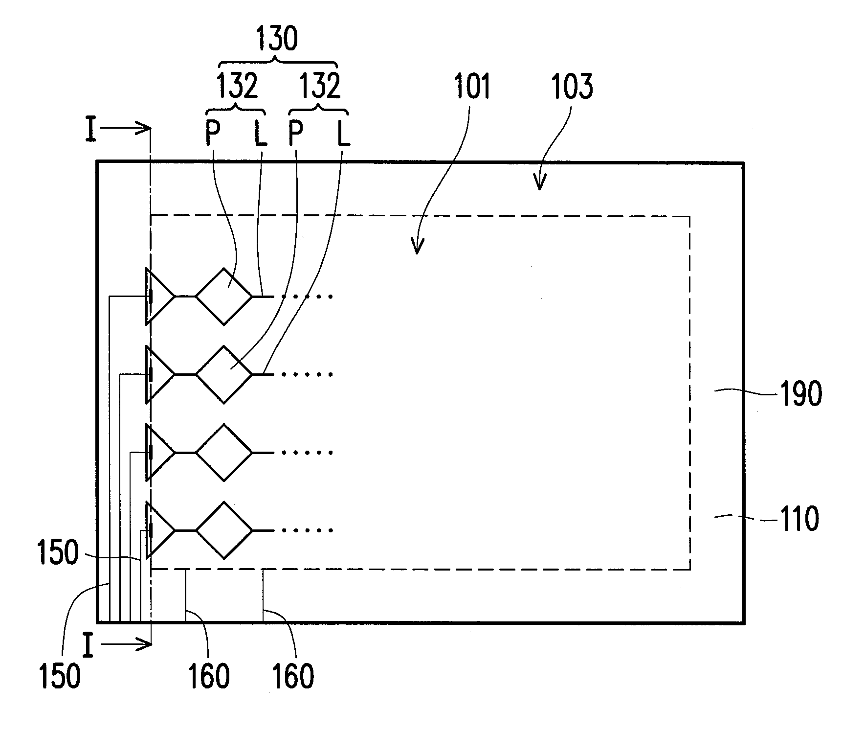
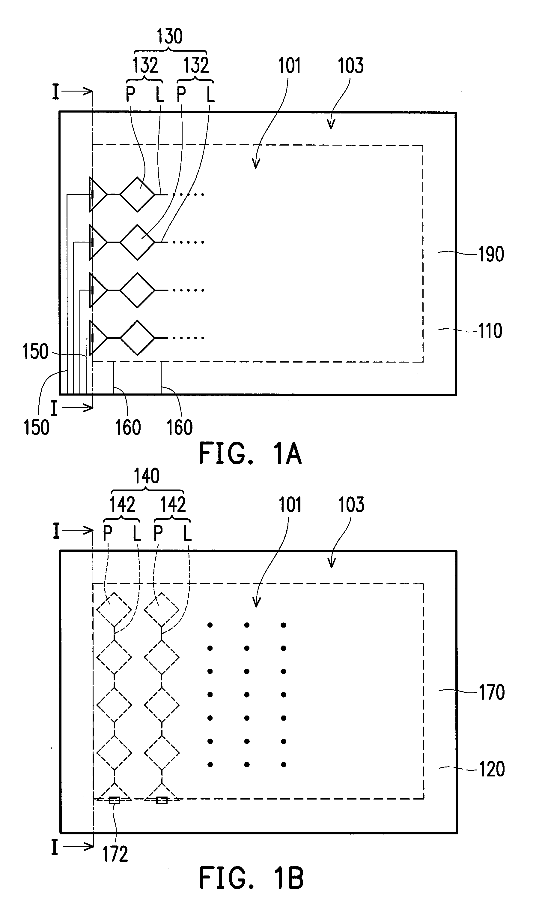
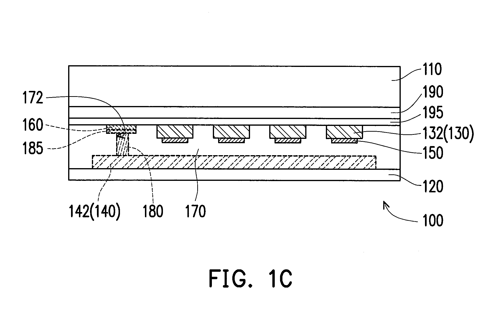
[0022]FIG. 1A is a top view of a first substrate of a touch panel according to an embodiment of the invention. FIG. 1B is a top view of a second substrate corresponding to the first substrate of the touch panel of FIG. 1A. FIG. 1C is a cross-sectional view of FIG. 1A and FIG. 1B along an I-I line. For simplicity's sake, a part of members are omitted in FIG. 1A and FIG. 1B. Referring to FIG. 1A, FIG. 1B and FIG. 1C, in the present embodiment, the touch panel 100 has a sensing region 101 and a periphery region 103 surrounding the sensing region 101. The touch panel 100 includes a first substrate 110, a second substrate 120, a first sensing electrode layer 130, a second sensing electrode layer 140, a plurality of first lines 150, a plurality of second lines 160, an optical adhesive layer 170, a conductive material layer 180 and a shielding layer 190.

[0023]In detail, the second substrate 120 is disposed opposite to the first substrate 110. The first sensing electrode layer 130 is dispos...


PUM

PropertyMeasurementUnit
conductiveaaaaaaaaaa
flexibleaaaaaaaaaa
anisotropic conductiveaaaaaaaaaa

Abstract

A touch panel including a first and a second substrates, a first and a second sensing electrode layers, plural first lines, plural second lines, a conductive material layer and a shielding layer is provided. The first and the second sensing electrode layers are respectively disposed on the first and the second substrates and located in a sensing region. The first and the second lines are disposed on the first substrate and located in a periphery region. The first lines connect to the first sensing electrode layer. The optical adhesive layer encapsulates the first and the second sensing electrode layers and the first and the second lines. The optical adhesive layer has an opening. The conductive material layer is disposed inside the opening. The second lines connect to the second sensing electrode layer via the conductive material layer. The shielding layer is located above the first and the second lines.

Description

CROSS-REFERENCE TO RELATED APPLICATION[0001]This application claims the priority benefit of Taiwan application serial no. 101124812, filed on Jul. 10, 2012. the entirety of the above-mentioned patent application is hereby incorporated by reference herein and made a part of this specification.BACKGROUND[0002]1. Technical Field[0003]The invention relates to a touch panel and a manufacturing method thereof. Particularly, the invention relates to a touch panel and a manufacturing method thereof and a touch display panel.[0004]2. Related Art[0005]Along with booming development of electronic technology, and popularisation of wireless communications and networking, various electronic devices gradually become indispensable tools in daily life. However, a commonly used input / output (I / O) interface, such as a keyboard or a mouse has a certain degree of operation difficulty. Comparatively, a touch panel is an intuitive and simple I / O interface. Therefore, the touch panel is generally used as a...

Claims


Application Information

Patent Timeline
Patent Type & Authority Applications(United States)
IPC IPC(8): G06F3/041H05K13/00
CPCG06F2203/04103Y10T29/49105G06F3/0445G06F3/0446
Inventor HSIEH, YUN-NANCHEN, LIN-AN
Owner E INK HLDG INC
Why Eureka
Try Eureka